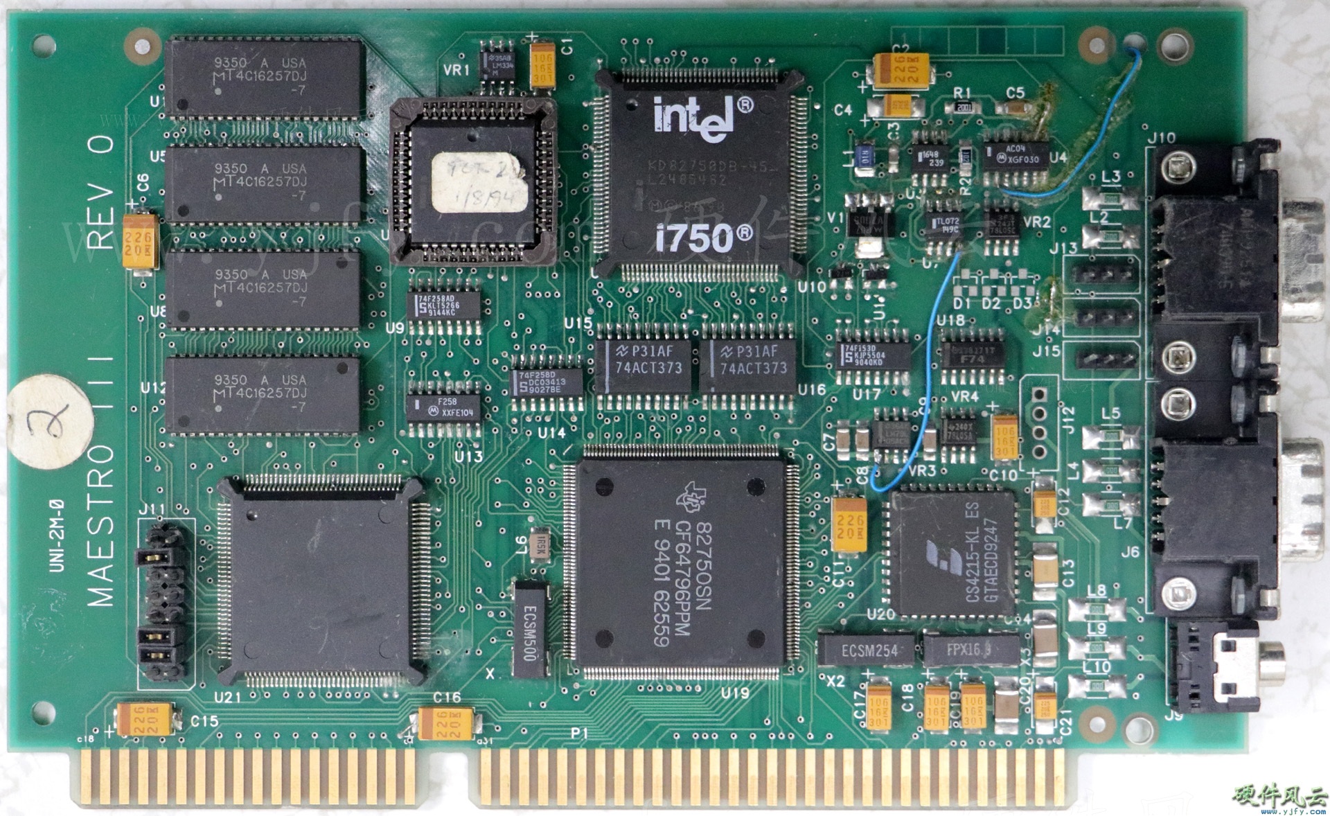
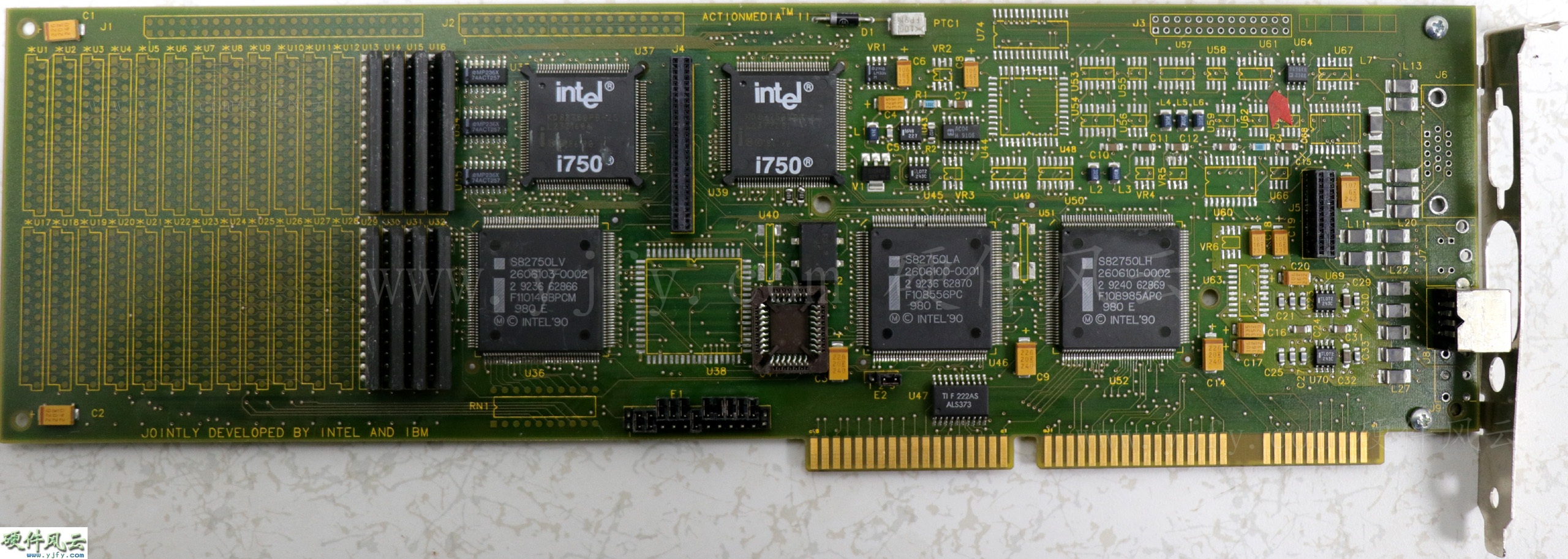
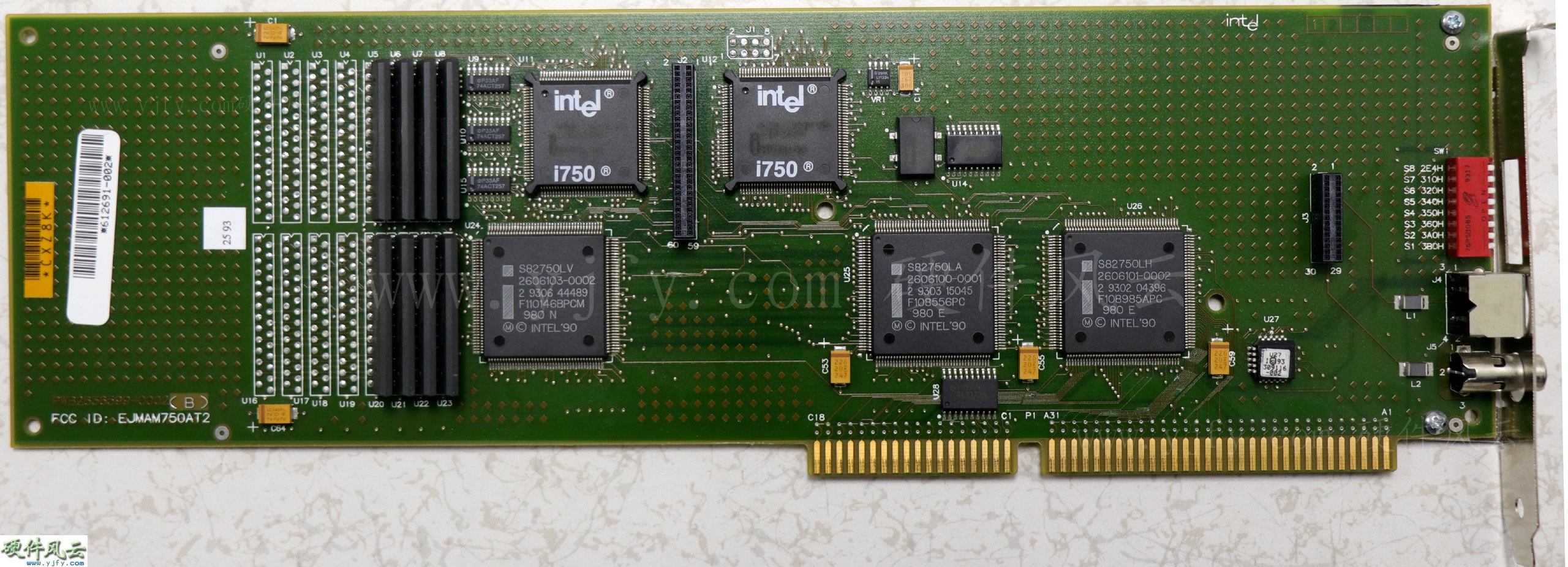
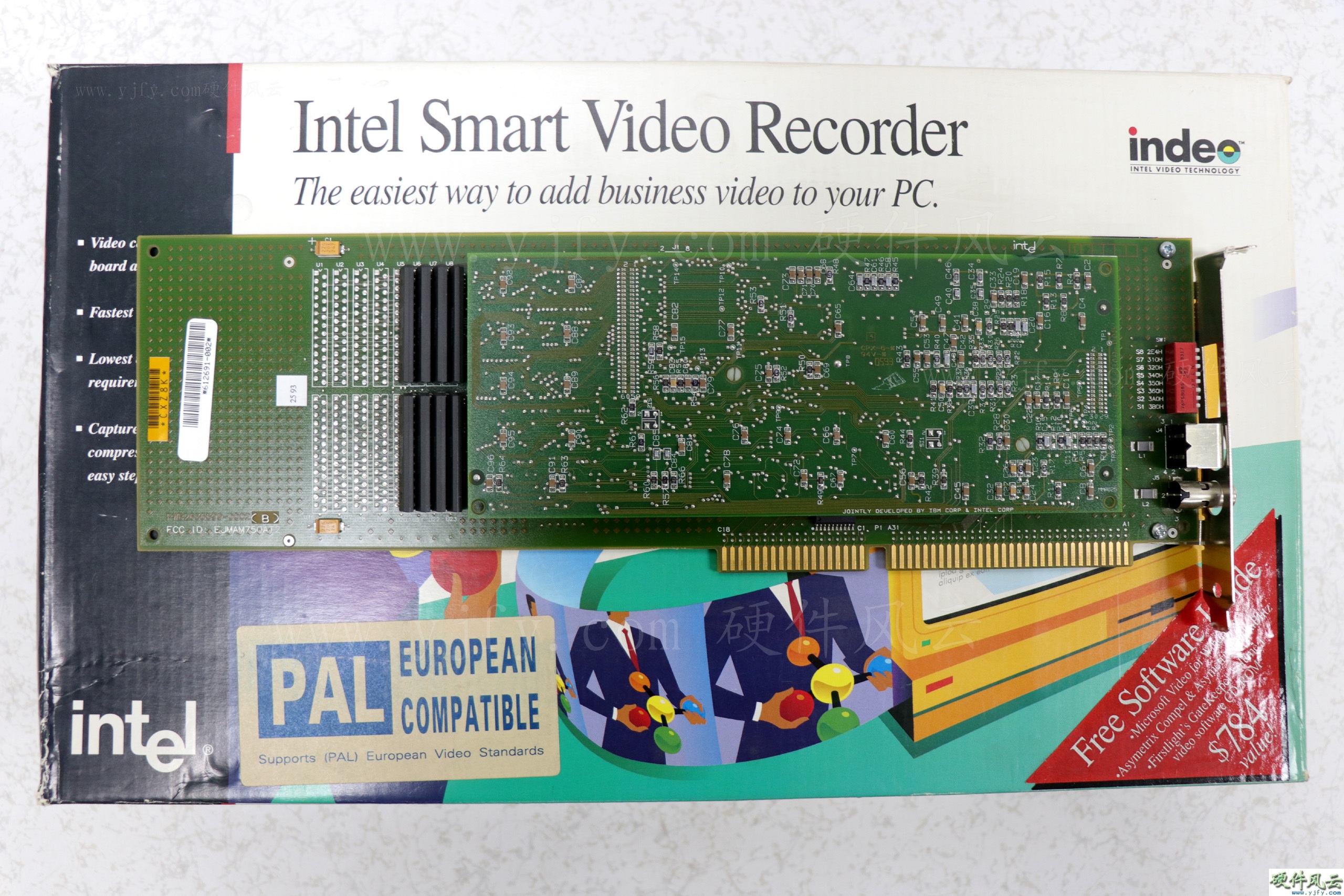
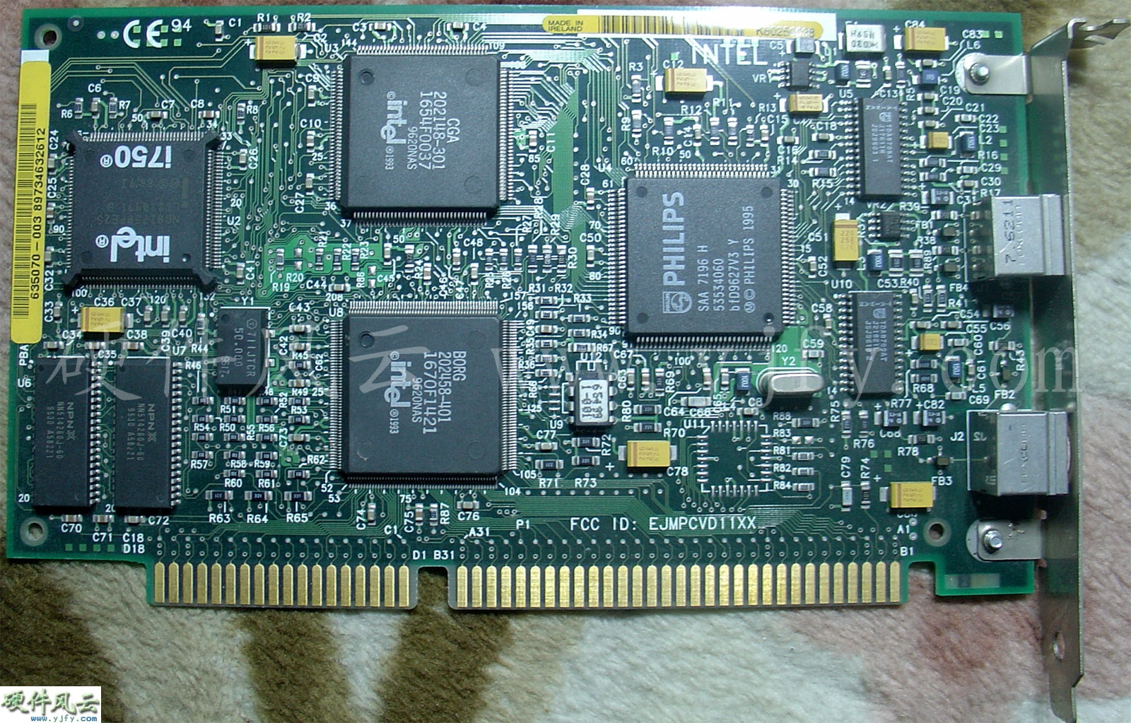
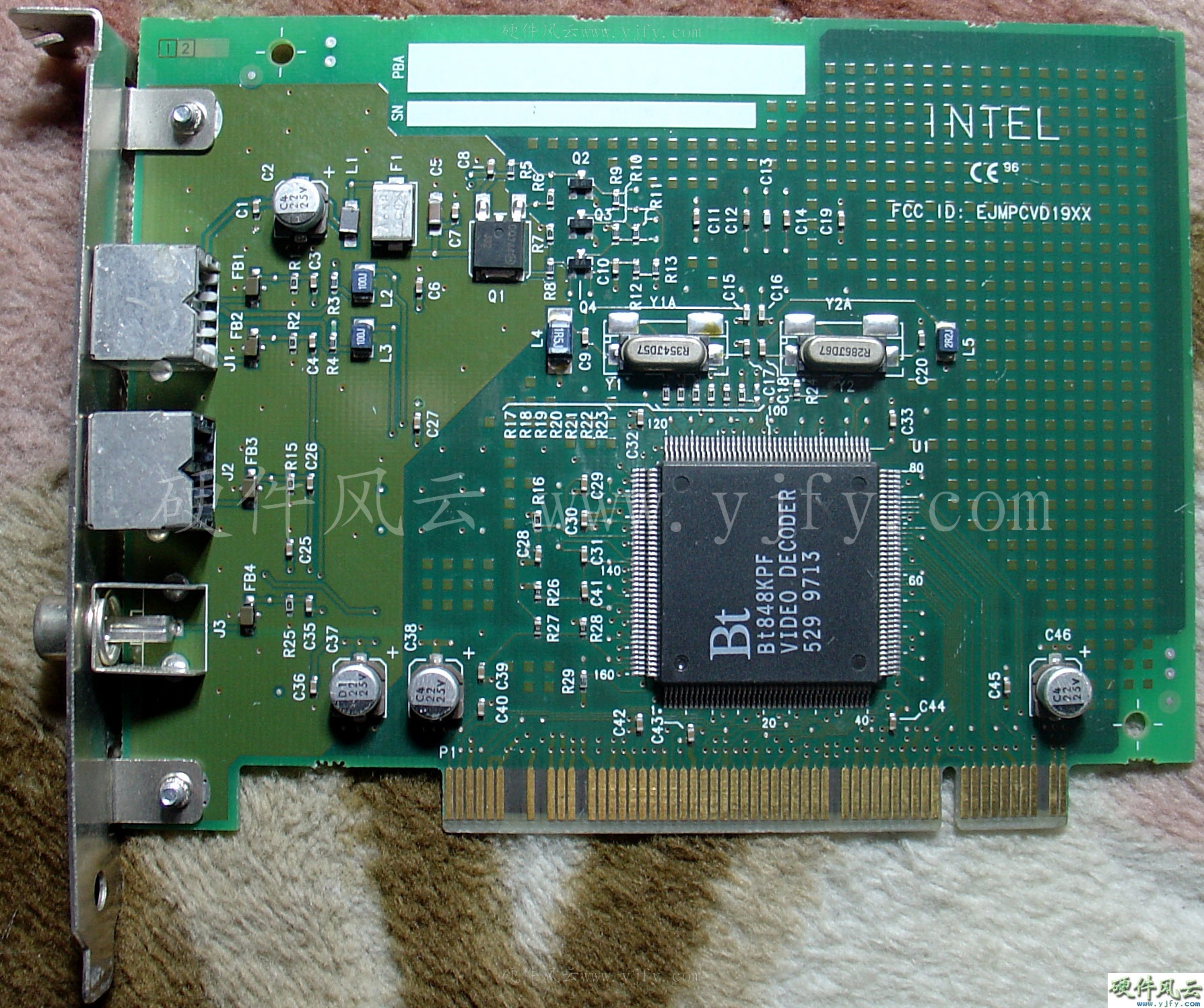
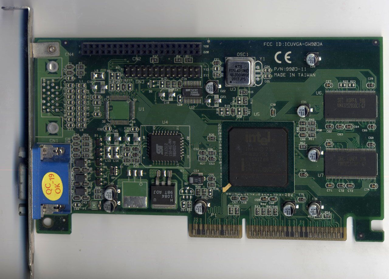
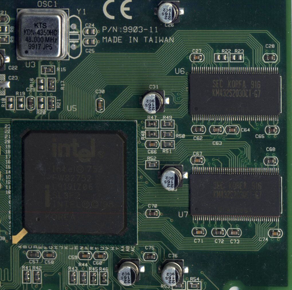
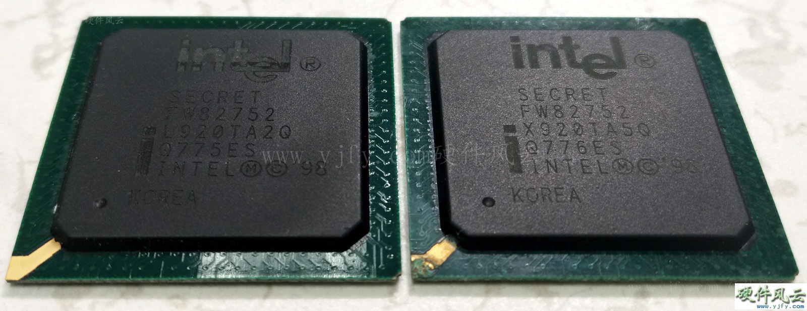
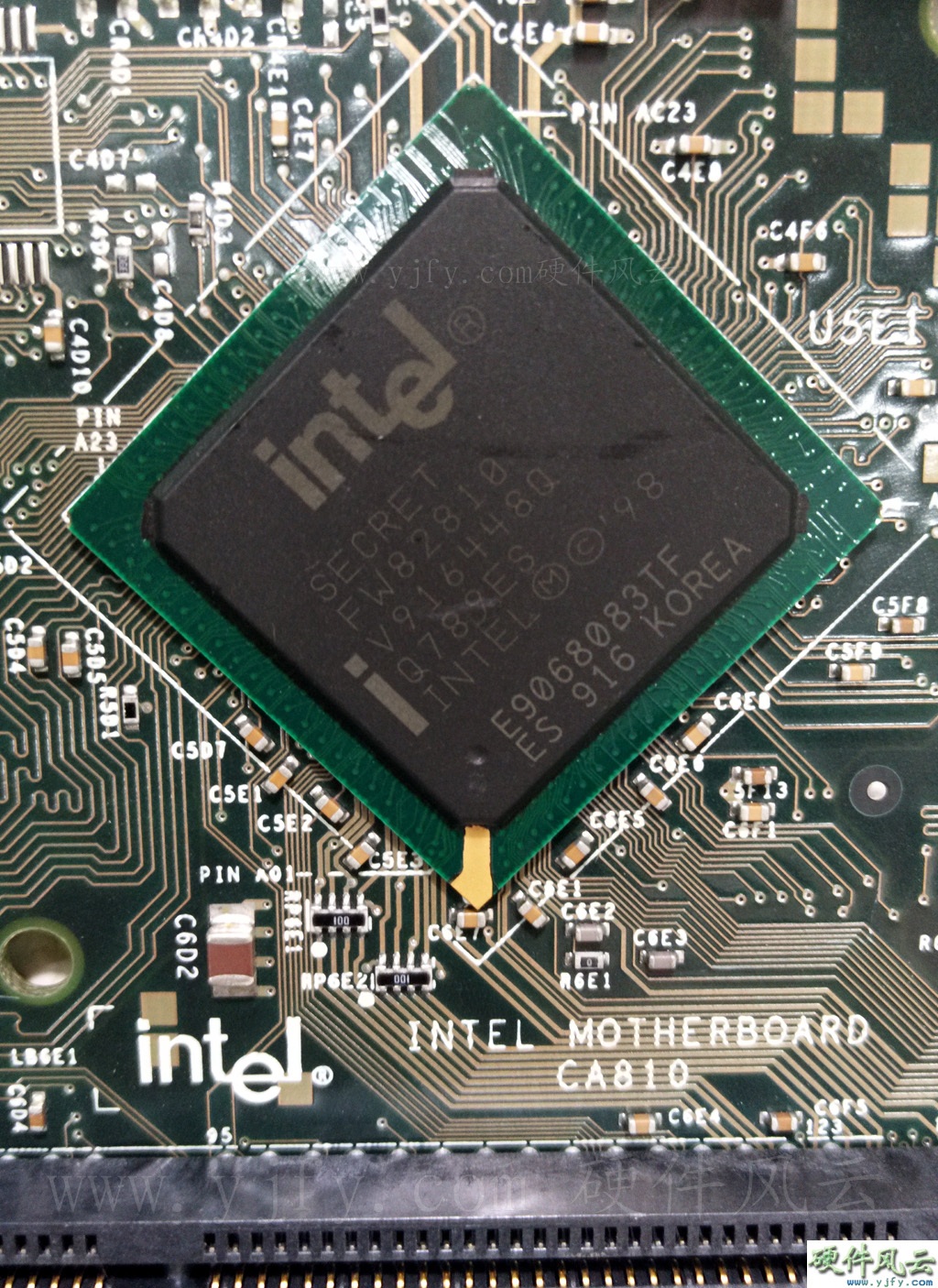
• Please review our updated Terms and Rules here

History of Intel graphics card

  2.4 i750PD Chip
  ACTIONMEDIA III did not routinely develop the i750's third-generation i750PC/DC chip, resulting in the vacancy of the i750PC/DC numbering chip. The fourth generation is the i750PD (Video Compression Processor) chip.
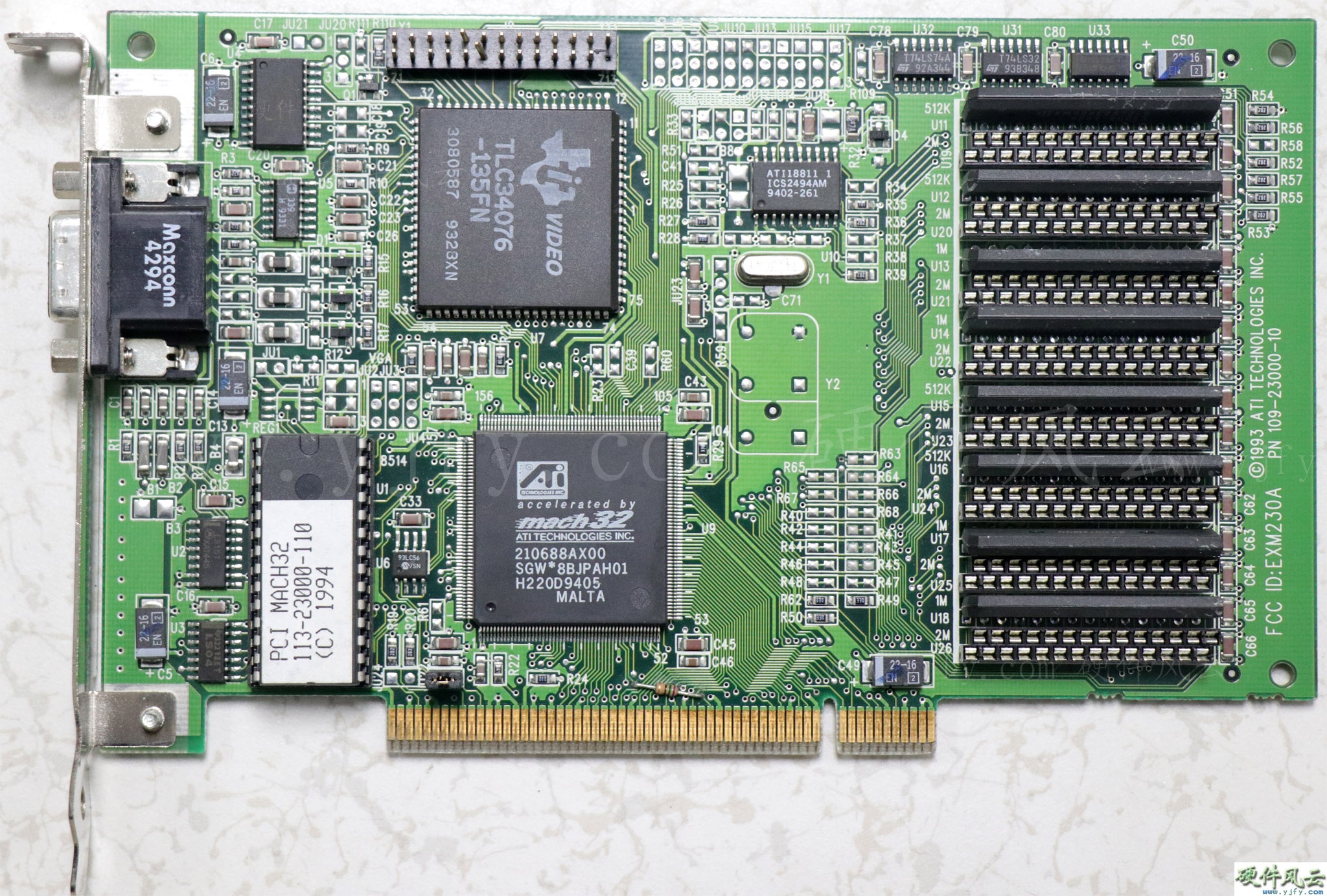
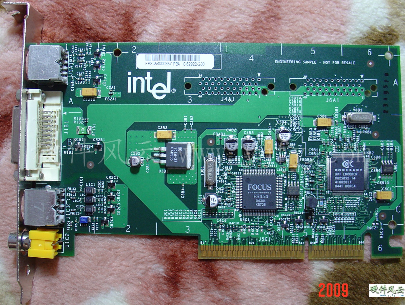
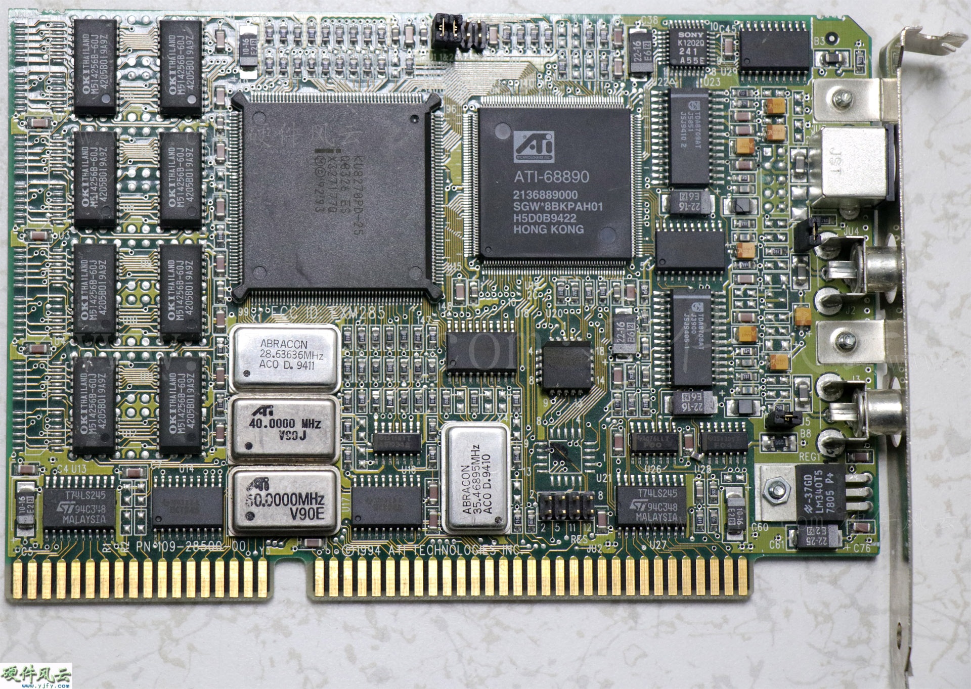
   On November 15, 1993, ATI announced the Video basic capture card, which uses Intel's low-cost i750PD and ATI's ATI-68890 video capture chip. The chip below shows the ATI Video basic capture card is ES, the chip is labeled KU8270PD-25, it seems to be marked incorrectly, it should be KU82750PD-25.
  ATI Video basic capture card Qualified Product
  
EXM285.jpg
 
  2.5 MAESTRO series
   The late stage of the i750 chip graphics project,lintel did not completely abandon the research and development of the i750 chip follow-up products, turned to simplified functions, low-cost video daughter cards and committed to selling i750 series chips to large companies such as ATI and Creative.
   MAESTRO III Evaluation board
  
MAESTRO_III.jpg

   The MAESTRO III card has i750DB, i750SN and a chip without any label. This chip without any standard should be the next generation chip, because at this time Intel can not make the i750PB into a wordless version of ES. The i750SN chip should be the F122164PPM on the QUARK chip board.As can be seen from the date of the components used on the card, the i750PE chip was made in early 1994. For some reason, the final product of such a card structure has not been seen, or only the i750PE chip is evaluated, and the chip is prepared for the Smart video Recorder series.
 
  2.6 Smart video Recorder series
  In the late stage of the ACTIONMEDIA II graphics card, INTEL removed the graphics display function of ACTIONMEDIA II and turned it into a Smart video Recorder series video capture card. Smart Video Recorder literally means a smart recorder that captures and compresses video analog signals into digital video files for playback and editing.
  2.6.1 Smart video Recorder Product Evaluation board
  Smart video Recorder Product Evaluation board
  
ACTIONMEDIA_II_4592_ES.jpg

  2.6.2 Smart video Recorder Qualified Product
   Smart video Recorder Qualified Product
  
Smart_video_Recorder.jpg

  
Smart_video_Recorder_5.jpg
 
  2.6.3 Smart video Recorder pro
  Although the ACTIONMEDIA III and MAESTRO projects were aborted, the BORG, CGA and i750PE chips were provided for the Smart video Recorder pro.Creative has similar products available.
  SMART VIDEO RECORDER PRO Qualified Product
  
EJMPCVD11XX.jpg

   2.6.4 Smart video Recorder III
    Smart Video Recorder III does not use INTEL's i750 series chips, nor is it the ISA/MCA interface used by INTEL's first-generation graphics cards. A PCI-based Smart Video Recorder III video card made an inexplicable end to INTEL's first-generation graphics card in 1996.
  Smart video Recorder III Qualified Product
  
EJMPCVD19XX.jpg

   Intel's first-generation graphics project began in 1989 with ACTIONMEDIA, and finally in 1996 the Smart Video Recorder III, which lasted eight years. Because the products are rarely seen on personal computers, their popularity is so low that they are forgotten.
 
  3. 2 years of granding (1997-1998)
  Intel's first generation of discrete graphics is based on the i750 chip ISA/MCA interface graphics card, the second generation of discrete graphics is the well-known AGP interface 3D graphics. It’s weird, it’s not a graphics card based on Intel’s PCI interface. Perhaps Intel is extremely confident about the i750 chip-based graphics card and missed the era of PCI graphics.
  3.1 PCI version graphics card
  Although Intel has not officially launched PCI discrete graphics, there are still some Intel-related PCI graphics cards.
  3.1.1 Purchase graphics card
  In the era of ISA graphics, Intel has used VIDEO 7 INC graphics cards. Intel, Intel also directly purchased graphics cards from PCI cards, such as ATi graphics cards.
  
mach32_1.jpg

  
mach32.jpg

  3.1.2 ODM graphics card
   In the era of PCI graphics, Intel has a partnership with VIDEO 7 INC. SPEA Software AG acquired VIDEO 7 INC. SPEA Software AG gives Intel ODM PCI graphics cards.
  
intel_928.jpg

  3.1.3 Acquisition of graphics card company
   In order to acquire the relevant technology, in July 1997, Intel acquired Chips & Technologies, which was the leader in 2D display design and R&D. Intel's move is not only to avoid the embarrassing situation that no graphics card is available in the era of PCI graphics, but also a sign of vigorously entering the graphics card market.
   DKHIQV-PCI Development board
  
DKHIQV-PCI_BOARD.jpg

   This DKHIQV-PCI Development board has an "INTEL" label.
 
  3.2 i740 chip series graphics card
  Intel's second-generation discrete graphics card began in the second half of 1997 with the AGP interface graphics card developed by Intel and Real3D, codenamed "Auburn", and was released in January 1998.
   The i740 is manufactured in a 0.35 micron process and is a 64Bit graphics core with a core operating speed synchronized to the AGP bus at 66MHz. The i740 is the first true AGP 2X graphics card. Supports up to 8MB of SGRAM/SDRAM memory. The pixel fill rate is 55M Pixels/s, the triangle generation speed is 0.5-1M Trianglws/s triangle generation speed is 5-10 million per second, and the 203MHz RAMDAC is built in. Although the i740's 2D speed is average, its 3D performance is not bad, and it can fully support hardware DVD playback.
  
  3.2.1 INTEL740 Evaluation board
  The following picture shows the intel i740 chip evaluation board. The right side of the front side of the PCB on the graphics card is marked with the "INTEL740 Evaluation board". The PCB date was 3497 and it appeared before August 1997.
   INTEL740 Evaluation board
  
INTEL740_E_1.jpg

  Although the i740 chip was developed by Real3d, the chip is marked with Intel's logo. It can be seen that intel pays attention to the i740.
  3.2.2 Real3D StarFighter-ISV Evaluation board
   This is the chip evaluation board of the i740 chip SDRAM memory version. It seems that Real3D and Intel are responsible for chip evaluation of SDRAM and SGRAM versions respectively.
   StarFighter-ISV Evaluation board
  
StarFighter-ISV.jpg
 
  3.2.3 Intel740 Reference board
  The front right side of the PCB on the Intel 740 graphics card is labeled "INTELi740 reference board". Intel had planned to let other manufacturers make graphics cards according to this reference design. In fact, based on cost considerations, no one vendor used this luxurious design, and even Intel itself launched Express 3D graphics cards to be streamlined and streamlined.
   INTELi740 reference board
  
intel740_reference_board_1.jpg
 
  3.2.4 Express 3D
  On April 15, 1998, Intel officially released the express 3D graphics card, which is the first generation of Intel independent graphics card commonly used on the Internet. After reading the previous information, I think you will only agree that it is the first generation of Intel 3D graphics card.
  3.2.4.1 Express 3D Evaluation board
  Product evaluation board for Express 3D, date of manufacture 9804.
   Express 3D Evaluation board
  
Express_3D_SGRAM_ES_2.jpg

  3.2.4.2 Express 3D Test board
     This Express 3D graphics card is a Test board that intel completes the design and is in trial production, which is no different from the official retail product. Compared with the Express 3D graphics Evaluation board, you can see obvious changes from the picture: the core version of the graphics card is upgraded, the BIOS version is updated from the 002 version to the 003 version that is consistent with the official product, and the failed certification is reduced from four to two. The two vertical rows of resistors under the fan interface change from full to full soldering. Also, the date of this card PCB is 98 years and 09 weeks, and the official release date of Express 3D graphics card is April 15, 1998, which is equivalent to 15 weeks in 1998. The test for the media evaluation agency is mainly the Test board before the release date.
  Express 3D Test board
  
express_3d_4m_sgram_es.jpg
 
  3.2.4.3 Express 3D SGRAM
     The first civilian-grade graphics card with fan cooling.
     Express 3D Qualified Product
  
Express_3D_sgram.jpg

     The shrink film of the Express 3D graphics card has an intel logo, as if opening the box would destroy its integrity. Take a look at the rabbit brother's collection.
  
i740.jpg

  (Source: t-cpu.com)
     Compared to the ACTIONMEDIA 750, the box of the Express 3D graphics card is really too small.
  
intel_box.jpg

  3.2.3.4 Express 3D SDRAM
   Express 3D SDRAM memory version.
  Express 3D SDRAM Qualified Product
  
Express_3D_sdram_2198.jpg
 
3.3 i752 chip series graphics card
On April 27, 1999, Intel released i752 (codename: Portola) and i754 (codename: Coloma). The i752 uses a 128Bit graphics core with a core frequency of 100MHz and a maximum memory support of 133MHz and a maximum of 16MB. The pixel fill rate is 100M Pixels/s, the triangle generation speed is 3.3M Trianglws/s, and the built-in 250MHz RAMDAC. It adopts dual pixel pipeline to support environmental atomization, single-cycle texture synthesis, 16-bit Z-buffer, bump map, texture compression and other technologies. In addition, it has improved graphics acceleration performance that can be accelerated for various graphics streaming formats at the time. The difference between the two chips is that one supports AGP2× and one supports AGP4×.
I752 and i754, this is just an improved product of the i740 with limited performance. The i752 chip shipments are limited, and only a small number of graphics cards have been produced by Gainward. The i754 chip project was withdrawn.
3.3.1 Intel752 Reference board
The display chip date of this i752 reference board is 9917.
Intel752 Reference board
intel752_reference_Board.jpg
 
  3.3.2 Gainward i752 commemorative card
   At Computex 99, intel sent the i752 graphics card to 50 lucky viewers, which is the Gainward i752. The only symbolic sale of the i752 chip graphics card. After reading the following pictures, you will understand why intel does not sell i752 chips.
  Gainward i752 commemorative card
  
i752.jpg

  i752 Chip
  
i752_1.jpg

  
   The i752 chip above is a formal chip with a date of 9919.
  i752 chip engineering sample
  
i752_9920.jpg

  The above picture is a sample version of the i752 chip project submitted by friend NEST, dated at 9920, later than the official version of the Gengyu i752 commemorative card, 9919. It shows that the official version of the chip is not perfect, there are many problems, just intel in order not to jump the ticket, only to sell a very small number of i752 official chips. Because Intel has no energy to solve the problem after it becomes a graphics card, why? And listen to the next decomposition.
 
  4. 20 years of growing(1999-present)
     The I740 chip graphics card is undoubtedly more successful, but it is at the low end in the graphics card market. At this time, the 3D graphics card market is full of smoke, INTEL enters the 3D graphics card market by buying and buying, Intel technology deposition is limited, technology integration, innovation takes time, can only find another way.
  On February 20, 1997, Cyrix launched the Media GX chip of the IT industry's first chip integration solution (All in One). This epoch-making concept, "Integration," was later understood by Intel and introduced an "Integrated Graphics" solution in early 1999. On April 26, the i810 chipset with integrated i740 display core was released. The i810 has achieved unprecedented success in the market and has contributed greatly to the popularity of integrated chipsets.
  4.1Integrated Graphics
  The i740 and i752 display cores are integrated into the north bridge chip of the i810/815 motherboard chipset, which shows that the core occupies part of the main memory of the computer during operation, which reduces the performance of the computer, but the cost and power consumption of the entire platform is lower.
  4.1.1 i810 Series
  The question about whether the i810 integrates the i740 or the i752 display core has been debated. The display chip date of the i752 reference board in this paper is 9817, and the date of the i810 North Bridge chip integrated with the display core on the CA810 motherboard is 9816. It is impossible for the i810 chip to integrate the i752 display core, which is also in the engineering sample stage, and should be the i740 display core.
  The i810 series has i810, i810E and i810E2.
  4.1.1.1 i810Chip
  The i810 chip was released on April 26, 1998, and the first cluster display board CA810 was released on June 25.
  i810 chip engineering sample
  
CA810_2.jpg

  CA810 Mainboard Engineering Sample
  
CA810_3.jpg
 
  4.1.1.2 i810EChip
  Released on September 27, 1998. The difference between the i810E chip and the i810 chip is to support the 133MHZ FSB.
  This unknown brand-name motherboard uses a rare i810E engineering sample chip.
  i810E chip engineering sample
  
810E.jpg

  
810E_1.jpg
 
  4.1.2 i815 Series
  The i815 chip has built-in i752 display chip and adds digital video signal output port (DVOP). There are four kinds of i815, i815E, i815G and i815EG.
  4.1.2.1 i815 Chip
   Released on June 19, 2000, the display core is the final result of the i752 graphics card project.
  i815 chip engineering sample
  
D815BN_2.jpg

  D815BN Mainboard Engineering Sample
  
D815BN.jpg
 
  4.1.3 Extreme Graphics Series
  
  In 2002, Intel introduced the i845G/E chipset with integrated "Extreme Graphics", which has significantly improved performance compared to the previous generation. The core frequency is 200MHz in the i845G, and the core frequency is 266MHz in the i845GE. The performance is close to that of Nvidia. Geforece2 MX 200, Extreme Graphics supports DVMT technology, which can dynamically call memory from the system, from the initial call 8MB to call 48MB.Products are i845G, i845GL, i845GV, i845GE.
  4.1.3.1 i845G
  i845GE Chip
  
D845GERG2_2.jpg

  D845GERG2 Mainboard
  
D845GERG2.jpg

  4.1.3.2 ADD expansion card (Advanced digital display)
   The ADD expansion card is not a stand-alone device. It must work in conjunction with the Intel Graphics Memory Controller Hub (GMCH) to provide high quality digital signal output. It provides an external graphics processing engine via a 1.5v AGP interface that provides digital signal output.
  Intel's PB C58792-002 ADD card adopts full-height design and supports DVI/video input and output. It is used in 845G series chipset motherboard. This card can output integrated graphics to the LCD through the AGP interface of the motherboard, and add extra Video input and output functions.
  PB C58792-002 Engineering Sample
  
PB_C58792-002.jpg
 
  4.1.4 Extreme Graphics II Series
   Intel has improved on Extreme Graphics and released Extreme Graphics II. Products are i865G, i865GV.
  i865GV Chip
  
MS-7101_2.jpg

  MSI MS-7101 Mainboard Engineering Sample
  
MS-7101_1.jpg
 
  4.1.5 Graphics Media AcceleratorSeries
  On June 21, 2004, GMA (Graphics Media Accelerator) Intel graphics chip was born. GMA is Intel's built-in graphics core product line from 2004 to 2008. Products are i910, i915, i945 series and so on.
  i945 Chip Engineering Sample
  
MS-7161_2.jpg

  MSI MS-7161 Mainboard Engineering Sample
  
MS-7161.jpg
 
  4.2 CPU with integrated graphics
  On the afternoon of January 8, 2010, Intel held a new Intel Core Launch Conference in Beijing. Intel officially released the latest revolutionary products worldwide, based on the new 32nm process Core i7, i5, i3 processor products. The Core i5/i3, which uses the Westmere architecture and is code-named Clarkdale, pioneered the integration of processors. It is the first CPU integrated with a GPU graphics core. The CPU is integrated with the GPU chip for the first time.
   Here are a few representative Core processors. 
  4.2.1 Core 1st generation
  
  The new generation Core i3/i5 processor, code-named Clarkdale, is packaged on the same substrate as the CPU. Although the CPU/GPU is packaged on the same substrate for the first time, the CPU part and the GPU part are independent. The CPU part adopts the 32nm process, and the GPU part adopts the 45nm process. The name is changed from GMA to HD Graphic's GPU core frequency. At 733MHz, performance is up to 50% higher than the previous generation GMA X4500HD. Although Clarkdale has not yet fully integrated the two cores of CPU and GPU, it is already a big breakthrough.
  
broken.jpg

  
i5.jpg

   (Image courtesy of http://www.expreview.com)
  
  Core i3 Desktop version engineering sample
  
i3_i5_ES.jpg

  Core i3 mobile version Engineering sample
  
i3_M_ES.jpg

  H55 chip motherboard
  
H55_2.jpg

  
H55.jpg
 
  4.2.2 Core 2nd generation
  
  In January 2011, Intel released a new Sandy Bridge architecture, which first merged the GPU chip with the CPU, and the built-in graphics core was upgraded to HD Graphics 2000/3000. There are 6 and 12 EU programmable shaders respectively.
  Opened Core i3 2100
  
i3-2100_1.jpg

  
i3-2100.jpg

  
  4.2.3 Core 4th generation
     Core 4th generation enhances display performance. Added eDRAM memory, supports 4K x 2K resolution, and upgraded high-speed video synchronization technology to make graphics images decode faster. The Intel HD Graphics 5200, codenamed GT3e, is called Iris Pro and has an eDRAM module that represents the strongest display performance of this generation.
    On the fourth generation of Core processor CPU board, there are two cores, the small core is eDRAM memory. From this Core CPU board, the CPU core is no longer monotonous, and there will always be other cores. 
    
i3_4_ES.jpg

    
i3_4_B_1.jpg
 
  4.3 Larrabee
  Intel's third-generation discrete graphics Larrabee was first announced at SIGGRAPH in 2008. Larrabee intends to build a stand-alone GPU and GPGPU using the x86 instruction set. It was originally expected that “Larrabee” will be launched in the third quarter of 2008 and officially released in 2009, but in fact there were engineering samples in 2009.
  
IMG_8796.JPG

  (Source: ZZC's collection)
  On November 4, 2009, Intel officially announced that Larrabee will not be released as a consumer GPU product. Instead, it will compete with Nvidia Tesla as a development platform for graphics and high-performance computing. In 2010, Intel completely canceled Larrabee.
   Larrabee without a DVI interface is no longer called Larrabee, it is a CPU.
  
intel_larrabee_engineering_sample_2.jpg

  
intel_larrabee_engineering_sample.jpg

  (Source: Collectibles from PCANG.com)
 
Back
Top