- VCF South West - June 14 - 16, Davidson-Gundy Alumni Center at University of Texas at Dallas
- VCF West - Aug 2 - 3, Computer History Museum, Mountain View, CA
- VCF Midwest - Sept 7 - 8 2024, Schaumburg, IL
- VCF SoCal - Mid February 2025, Location TBD, Southern CA
- VCF East - April 2025, Infoage Museum, Wall NJ
-
Please review our updated Terms and Rules here
- Forums
- Companies
- IBM Computers, PCs, Clones and Descendants
- PCs and Clones (XT and early AT class machines)
You are using an out of date browser. It may not display this or other websites correctly.
You should upgrade or use an alternative browser.
You should upgrade or use an alternative browser.
IBM 5170 restoration - PSU fixed, now RAM problems - SRAM replacement?
- Thread starter mrmanse
- Start date


sponaugle
Member
I did a few tests on my TYPE-1 5170 motherboard with 512K installed ( And J18 set for 512k)
First up is U64 Pin 12 (RAM0CAS), which shows normal traffic during idle operation.

Next up is U64 Pin14, RAM1CAS, showing activity because I was running a memory test that was working in that upper section of memory.

Here is Pin 7 on U64 (the input side) during a busy part of the memory test. This input side has quite a bit more noise present that is directly coupled from the other rapid signals. As well the scope ground pickup is quite long so that adds a lot of capture noise.

However, there are a few other observations - The RCAS1 signal coming out of U64 shows no activity when there is no direct RAM access to that region. These memory ICs support RAS only refresh, so you don't see activity on the CAS lines unless there is direct memory access. If you just boot up the computer, you will only see CAS activity during the memory test done by the BIOS.
I verified with my scope that if I , for instance, go into DEBUG and do a 'd 5000:0000', there is activity on the CAS1 line as the debugger reads each line of memory. This confirms that blocking that signal should prevent the bus drivers from changing direction, thus allowing all system memory to be on the ISA bus. I will confirm that as soon as I get a PCB back from production.
First up is U64 Pin 12 (RAM0CAS), which shows normal traffic during idle operation.
Next up is U64 Pin14, RAM1CAS, showing activity because I was running a memory test that was working in that upper section of memory.
Here is Pin 7 on U64 (the input side) during a busy part of the memory test. This input side has quite a bit more noise present that is directly coupled from the other rapid signals. As well the scope ground pickup is quite long so that adds a lot of capture noise.
However, there are a few other observations - The RCAS1 signal coming out of U64 shows no activity when there is no direct RAM access to that region. These memory ICs support RAS only refresh, so you don't see activity on the CAS lines unless there is direct memory access. If you just boot up the computer, you will only see CAS activity during the memory test done by the BIOS.
I verified with my scope that if I , for instance, go into DEBUG and do a 'd 5000:0000', there is activity on the CAS1 line as the debugger reads each line of memory. This confirms that blocking that signal should prevent the bus drivers from changing direction, thus allowing all system memory to be on the ISA bus. I will confirm that as soon as I get a PCB back from production.
Just to make some progress I mailed Mans recently. I asked him politely to join the discussion here again, or alternatively, respond to my mail. The mail address seems to still exist. Let's see...No, not yet, but happy to also reach out. I'll send you a DM and we can co-ordinate. It would be interesting to hear about a few of the decoding issues he had.
Sounds reasonable. For being able to follow, I asked DipTrace for a free Non-Commercial version, limited to 500pins. That should be sufficient, isn't it?I'm using DipTrace which is a particularly easy schematic and PCB tool...
sponaugle
Member
Oh yes, you can download the version that is the default trial and that might be sufficient. I"ll check the pin count.Just to make some progress I mailed Mans recently. I asked him politely to join the discussion here again, or alternatively, respond to my mail. The mail address seems to still exist. Let's see...
Sounds reasonable. For being able to follow, I asked DipTrace for a free Non-Commercial version, limited to 500pins. That should be sufficient, isn't it?
I started a new thread :
mrmanse
Member
Hi all!
I'm happy to learn about your interest in my work! Thank you Markus for letting me know about the revival of the thread, I'm sorry I didn't see it sooner.
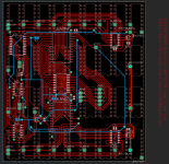
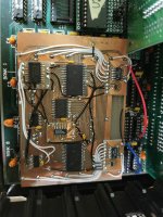
The IBM5170 SRAM replacement board was a very nice project, and although many details are dim to me now, I'd be glad to help. Attached are a photo with my working prototype (100% working, thoroughly tested). As you can see, it's heavily modded during the design process, and of course should not be duplicated as is. I did however prepare schematics and board layout for a more final version, which I never built, but I hereby release the design to the forum. It's free for any personal use, but a reasonable credit is much appreciated if used in any commercial products.
So, the schematic is untested, but based on my findings during development of the prototype. If I haven't made any misstakes it should work as is. If anyone decides to built it and finds that is doesn't work, I will of course assist. If so it could most likely be modified to work, like my prototype.
Please note! I'm not allowed to post the schematic/board because of forum restrictions files but I'd be happy to share them, along with the required library files. Just drop me a mail (you'll find it on the board pictured).
/Måns
I'm happy to learn about your interest in my work! Thank you Markus for letting me know about the revival of the thread, I'm sorry I didn't see it sooner.
The IBM5170 SRAM replacement board was a very nice project, and although many details are dim to me now, I'd be glad to help. Attached are a photo with my working prototype (100% working, thoroughly tested). As you can see, it's heavily modded during the design process, and of course should not be duplicated as is. I did however prepare schematics and board layout for a more final version, which I never built, but I hereby release the design to the forum. It's free for any personal use, but a reasonable credit is much appreciated if used in any commercial products.
So, the schematic is untested, but based on my findings during development of the prototype. If I haven't made any misstakes it should work as is. If anyone decides to built it and finds that is doesn't work, I will of course assist. If so it could most likely be modified to work, like my prototype.
Please note! I'm not allowed to post the schematic/board because of forum restrictions files but I'd be happy to share them, along with the required library files. Just drop me a mail (you'll find it on the board pictured).
/Måns
Attachments
Hello everyone,
I saw what was done in these designs, where you want to preserve the original DRAM memory control, which is one possible functional route to go.
At least, I am only going from what I could see in the PDF circuit diagram of Mans only.
This is definately the least invasive method of course, it all depends on what the plan is of course and what someone would be willing to modify which will differ.
I see that Sponaugle is using a different method to make his own decoders which is definately also minimally invasive which is appealing in its own way.
This thread caught my interest because I am currently working on a NCR PC-8 rev 0 which is basically a clone of the IBM 5170.
I got the PCB from Ebay without CPU, ROMs, CMOS clock and keyboard controller. (I hate it when they do that!)
And with only 256k of RAM on the PCB.
After a bit of work it's now working with a quadtel bios which is compatible with the IBM 5170.
I exchanged the PLCC CPU socket with a more modern one and used a Harris CS80286-16. and expanded to 640kb of DRAM.
I found that the mainboard only operates with the MC146818 and not with a DS12885, however it seems to work with a DS12887 so it is probably clock input related.
So far I ran a Norton NDIAGS comprehensive memory test without any errors so my DRAM appears to be Ok.
I can run DOS and windows 3.0 and tested patience for a while without crashes so the CPU is stable and so is the RAM and ISA bus.
So far so good, but then of course unfortunately there are some complications.
When I run any DMA operation, it disrupts the refresh or parity circuits which results in a parity check error and subsequent halting of the CPU.
I have also observed "internal stack overflow system halted" earlier as well.
Examples of where my mainboard crashes during DMA operations:
- floppy read/write access
- sound samples in WOLF3D game with Soundblaster Pro 2 - results in immediate freeze
The floppy drive is really an ideal DMA test for early discrete PCs such as these.
I have removed and tested the 8237 DMA controllers of the PC-8 mainboard in my XT, they are functional but the timing is not great.
I also found some sound glitches in WOLF3D but no actual crashes using these DMA controllers.
So I replaced both with better performing ones on the AT mainboard which worked well with floppy access and WOLF3D on my XT.
However this also didn't result in a stable DMA on the AT unfortunately.
My theory now is that the Harris CPU I used or something else in the system has different impedance from the original system which is throwing off the timing of the DMA control logic.
It's either that or something else is still defective. For example some of the programmable logic may have failed.
So I will need to remove and verify those too. This is a little tricky because I saw that the connection sequence is different from the IBM design.
I can't know because my mainboard was incomplete and not fully populated.
What I hope to achieve is to get a stable PC with this mainboard or a similar one which also can do DMA normally as originally designed.
This mainboard is of interest to me because I plan to design my own improved ATX version of this mainboard.
I did the same with the XT PC and integrated some useful interfaces into my PCB.
Anyone who likes to take a look can visit my website for reference.
Just to get an idea of what I am aiming for in my next project with a discrete AT design.
What I intend to do is somewhat different from the designs featured in this thread, because I plan to do away with the existing CAS and RAS circuitry and memory management completely.
And I also plan to remove the parity checking circuits.
I will only connect the /DACK0 to the ISA bus for certain cards which use it as a timing reference.
Since I will be using SRAM only, there will be no need for all these circuits on my design.
Also, when I use adapter cards I will pay attention that there is no DRAM on them which depends on mainboard logic to refresh.
However I don't plan to use such cards. If there is more memory possible, I will enable this using SRAM instead and include the SRAM on the mainboard anyway.
I did the same changes on my XT design, however of course this time it will be a slightly more involved process since the IBM AT design is somewhat more complex.
However, if you view it from the other side, to simply cut out the unwanted circuits which were designed for DRAM anyway, and design from the specifications rather than from these original memory map circuits, the process may hopefully be more easy in my case for what I intend to do.
I may make some errors which I will need to correct later on if there are any things I may have overlooked in my design changes.
In theory, DMA should work fine with SRAM since it also does on my XT PC.
That's why I need this PC-8 as a reference, and that's the only reason I bought this mainboard.
These discrete chipset PCBs are rare to find so I was happy to find this PC-8.
However I was not impressed by the bad European PCB assembly quality since the PCB in my case has been soldered to the slot connectors in a warped fashion.
These DMA troubles are not something I expected, but it may be processor-specific and a sensitive aspect of this design, similar to what I found with DMA controllers in my XT design.
I expect that during my process I may find an ideal method of memory mapping.
Perhaps this method will be of use to others here who want to make an ISA card to plug into their PC.
Definately some not too invasive mods should be possible to disable the DRAM control and parity checking altogether.
This will definately make the IBM AT PC more stable and future proof in my opinion.
For those also interested in this route I can update my progress here in this forum.
However I first need to tackle this DMA trouble which is difficult.
I may try a different CPU also which is more close to the original one of this mainboard.
Only when I achieve 100% stability on a discrete AT PCB I can proceed with my project.
I don't want to risk finding unrecoverable problems further on since there is considerable work involved to design and build this project.
If there is anyone here who has some experience with DMA troubleshooting of the 5170, or even the NCR PC-8 rev 0, or who could be helpful to me in any other way, I would appreciate any help or advice of what you have tried.
I did replace the U64 74ALS573 with a 74HCT one which didn't give me any improvement, except to see higher output amplitude which looks better on a scope.
On my XT I did get some improvement by changing logic types of certain ICs, the DMA control remains a difficult thing but I tackled it finally on my XT.
Definately programmable logic is much faster than TTL logic equivalents.
If I am on a wrong track to find the solution for these parity problems I would also appreciate any advice.
So far it's still theoretical until I find the true solution anyway.
When I make progress in my project I will report it here, perhaps the theory of design can inspire similar other designs as discussed here as well.
If I can't get the DMA to work properly I may remove all the DRAM circuits and wire in my own version using SRAM.
That may be an alternative route to achieve a stable reference system.
I have only studied the IBM 5170 designs for a few days so far, not nearly as in-depth as my previous XT design yet.
Anyway, any ideas would be appreciated, I hope I can find someone who is familiar with what I am experiencing with the DMA here.
Kind regards,
Rodney
I saw what was done in these designs, where you want to preserve the original DRAM memory control, which is one possible functional route to go.
At least, I am only going from what I could see in the PDF circuit diagram of Mans only.
This is definately the least invasive method of course, it all depends on what the plan is of course and what someone would be willing to modify which will differ.
I see that Sponaugle is using a different method to make his own decoders which is definately also minimally invasive which is appealing in its own way.
This thread caught my interest because I am currently working on a NCR PC-8 rev 0 which is basically a clone of the IBM 5170.
I got the PCB from Ebay without CPU, ROMs, CMOS clock and keyboard controller. (I hate it when they do that!)
And with only 256k of RAM on the PCB.
After a bit of work it's now working with a quadtel bios which is compatible with the IBM 5170.
I exchanged the PLCC CPU socket with a more modern one and used a Harris CS80286-16. and expanded to 640kb of DRAM.
I found that the mainboard only operates with the MC146818 and not with a DS12885, however it seems to work with a DS12887 so it is probably clock input related.
So far I ran a Norton NDIAGS comprehensive memory test without any errors so my DRAM appears to be Ok.
I can run DOS and windows 3.0 and tested patience for a while without crashes so the CPU is stable and so is the RAM and ISA bus.
So far so good, but then of course unfortunately there are some complications.
When I run any DMA operation, it disrupts the refresh or parity circuits which results in a parity check error and subsequent halting of the CPU.
I have also observed "internal stack overflow system halted" earlier as well.
Examples of where my mainboard crashes during DMA operations:
- floppy read/write access
- sound samples in WOLF3D game with Soundblaster Pro 2 - results in immediate freeze
The floppy drive is really an ideal DMA test for early discrete PCs such as these.
I have removed and tested the 8237 DMA controllers of the PC-8 mainboard in my XT, they are functional but the timing is not great.
I also found some sound glitches in WOLF3D but no actual crashes using these DMA controllers.
So I replaced both with better performing ones on the AT mainboard which worked well with floppy access and WOLF3D on my XT.
However this also didn't result in a stable DMA on the AT unfortunately.
My theory now is that the Harris CPU I used or something else in the system has different impedance from the original system which is throwing off the timing of the DMA control logic.
It's either that or something else is still defective. For example some of the programmable logic may have failed.
So I will need to remove and verify those too. This is a little tricky because I saw that the connection sequence is different from the IBM design.
I can't know because my mainboard was incomplete and not fully populated.
What I hope to achieve is to get a stable PC with this mainboard or a similar one which also can do DMA normally as originally designed.
This mainboard is of interest to me because I plan to design my own improved ATX version of this mainboard.
I did the same with the XT PC and integrated some useful interfaces into my PCB.
Anyone who likes to take a look can visit my website for reference.
Homebuilt 8088 Turbo XT ATX Mainboard – Revision 3
Website van Knaap IC waarop u diverse relevante thema's en ideeën kunt vinden aangaande ICT voor bedrijven. U vindt op deze website een praktische kijk op kwesties en problemen die zich in de ICT van bedrijven kunnen voordoen. Knaap IC levert ICT hulp en diensten in regio achterhoek.
www.knaapic.nl
What I intend to do is somewhat different from the designs featured in this thread, because I plan to do away with the existing CAS and RAS circuitry and memory management completely.
And I also plan to remove the parity checking circuits.
I will only connect the /DACK0 to the ISA bus for certain cards which use it as a timing reference.
Since I will be using SRAM only, there will be no need for all these circuits on my design.
Also, when I use adapter cards I will pay attention that there is no DRAM on them which depends on mainboard logic to refresh.
However I don't plan to use such cards. If there is more memory possible, I will enable this using SRAM instead and include the SRAM on the mainboard anyway.
I did the same changes on my XT design, however of course this time it will be a slightly more involved process since the IBM AT design is somewhat more complex.
However, if you view it from the other side, to simply cut out the unwanted circuits which were designed for DRAM anyway, and design from the specifications rather than from these original memory map circuits, the process may hopefully be more easy in my case for what I intend to do.
I may make some errors which I will need to correct later on if there are any things I may have overlooked in my design changes.
In theory, DMA should work fine with SRAM since it also does on my XT PC.
That's why I need this PC-8 as a reference, and that's the only reason I bought this mainboard.
These discrete chipset PCBs are rare to find so I was happy to find this PC-8.
However I was not impressed by the bad European PCB assembly quality since the PCB in my case has been soldered to the slot connectors in a warped fashion.
These DMA troubles are not something I expected, but it may be processor-specific and a sensitive aspect of this design, similar to what I found with DMA controllers in my XT design.
I expect that during my process I may find an ideal method of memory mapping.
Perhaps this method will be of use to others here who want to make an ISA card to plug into their PC.
Definately some not too invasive mods should be possible to disable the DRAM control and parity checking altogether.
This will definately make the IBM AT PC more stable and future proof in my opinion.
For those also interested in this route I can update my progress here in this forum.
However I first need to tackle this DMA trouble which is difficult.
I may try a different CPU also which is more close to the original one of this mainboard.
Only when I achieve 100% stability on a discrete AT PCB I can proceed with my project.
I don't want to risk finding unrecoverable problems further on since there is considerable work involved to design and build this project.
If there is anyone here who has some experience with DMA troubleshooting of the 5170, or even the NCR PC-8 rev 0, or who could be helpful to me in any other way, I would appreciate any help or advice of what you have tried.
I did replace the U64 74ALS573 with a 74HCT one which didn't give me any improvement, except to see higher output amplitude which looks better on a scope.
On my XT I did get some improvement by changing logic types of certain ICs, the DMA control remains a difficult thing but I tackled it finally on my XT.
Definately programmable logic is much faster than TTL logic equivalents.
If I am on a wrong track to find the solution for these parity problems I would also appreciate any advice.
So far it's still theoretical until I find the true solution anyway.
When I make progress in my project I will report it here, perhaps the theory of design can inspire similar other designs as discussed here as well.
If I can't get the DMA to work properly I may remove all the DRAM circuits and wire in my own version using SRAM.
That may be an alternative route to achieve a stable reference system.
I have only studied the IBM 5170 designs for a few days so far, not nearly as in-depth as my previous XT design yet.
Anyway, any ideas would be appreciated, I hope I can find someone who is familiar with what I am experiencing with the DMA here.
Kind regards,
Rodney
I have traced back my DMA parity crashes, actually it appears that it's not coming from the DRAM parity check circuits at all.
The parity flipflop U86 (74F75) is switched on via the preset input by a pulse from ENB_RAM_PCK, which comes from IO port U127 (74ALS175).
There, XD2 (logic 1) is clocked through U127 briefly once and then cleared again by PORTB_WR which comes from IO decoder PROM U115.
I believe this is a secondary mechanism to signal error conditions which warrant an NMI to halt the CPU.
It's probably the BIOS or DOS signalling to the CPU that something went wrong in a DMA transfer.
So apparently the problem originates from the DMA procedure itself and has nothing at all to do with RAM parity and is not throwing off the refresh either.
The BIOS only writes this "parity" message because of the NMI going active on the CPU which is normally a parity error from the parity circuits.
I get a blank screen with only: "Parity Check 1 8FC0", but I am skeptical that 8FC0 has any significant meaning to indicate anything relevant.
I googled this but found nothing that contains this 8FC0 code which is consistent after several tests.
Anyway, this information might be useful for others who are seeing parity errors appear.
You can check if it's a real parity issue by monitoring the preset input pin 10 of U86.
If there nothing happens while you get a parity error, it's an actual parity problem.
But it may be a different issue if the preset of U86 is toggled.
I hope I can solve this problem and get a stable reference system so I can continue designing my new ATX 80286 mainboard.
I will definately share my future memory control circuits if anyone is interested later on.
Anyway, if anyone else has had any experience with this problem from DMA halting / freezing on the 5170 or similar system, I would really appreciate to read about it.
Hello everyone,
I have started a new thread about my DMA problem here:
I would appreciate any help and hope I can find someone who has more in-depth experience with this DMA problem and this type of mainboard.
Perhaps someone who has tried other CPUs on this mainboard for example.
Kind regards,
Rodney
I have started a new thread about my DMA problem here:
I would appreciate any help and hope I can find someone who has more in-depth experience with this DMA problem and this type of mainboard.
Perhaps someone who has tried other CPUs on this mainboard for example.
Kind regards,
Rodney