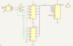
I should have posted this a week ago, but I had no time to redo the schematic until today. I haven't retraced the parts in my board since last week so take this as a grain of salt.
The Datamaster has two clock sources for the CPU and three for the video subsystem. The latter can work at 18.432MHz or 18.2MHz if the European switch is set - the third source hasn't been identified yet. Two components receive the selected signal: the video shift register and a 74LS174 configured as a shift register, which samples an unidentified signal and feeds it to the 8275 as a clock.
The CRTC has two outputs to signal attributes and the s/23 uses them to select the value to the character ROM or another one generated by a 74LS139 and a couple of NOT gates. The result is fed to the video shift register and NANDed with something.
There is still a lot of work to do. I also feel something is wrong as the 139 also controls the select signal of the 157s...
