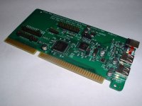
ARSTech makes ISA (and PCI) bus expanders that run as a USB slave device for machines that don't have either type slot. Not much help. What people want is the other way around.
I'm actually starting to tackle this project. However it's a spare time thing and that may not be much as I'm probably switching jobs in 2-3 weeks. My original scope was pretty pie in the sky - embedded MCU running Linux with a full USB stack supporting various USB classes - audio, HID, MSI, 802.11 network - being emulated as popular legacy equivalents - SB/GUS, game port/serial mouse, IDE disk/cdrom, NE2K/3C309. And the original scope also included adding a Super I/O chip for native floppy, 2S, 1P (bi, ECP/EPP), 1G, MPU-401, etc, an AC'97 codec, plus lower and XMS memory fill-in to 16MB of zero wait state RAM, and a real-time clock. (see what I mean about feature creep?)
However I've recently scaled back the scope significantly for round 1 to just USB MSI to IDE disk emulation and possibly CD-ROM support; along with serving up a controller BIOS from an SPI flash chip. It should allow for a 2 layer half height half length 16 bit ISA board (8 bit slot compatible) that supports emulation of basic IDE PIO and DMA modes. And the Vinculum-2 SDK seems robust enough that I can get away with not having to do a generic end-point queuing engine plus add a full USB software stack on the MCU. I can just handle everything at a block level over a simple fifo. My price point on components is now sitting at $~45 in unit quantity 1 (<35 for 25+), the PCBs are at $5-35 depending on final process requirements and quantity, back-plates are still up in the air, I can solder everything with equipment I already have (for a minimal assembly comp)... with the ultimate goal of a sub-100 dollar price point.
I've designed an ISA carrier board for a Lattice CPLD breakout board, FPGA eval board, and a Vinculum-II eval module and ordered the full parts kit. Should be here Wednesday so I can fit parts to to-scale pads before I order PCBs on Sat/Sun. The CPLD primarily is for a ISA to LPC bridge and has all 80+ ISA signals buffered into it with FETs (the idea was to play around as a busmaster eventually). It also has an additional 512 SRAM and 4MB SPI flash for an optional 8-bit soft-core MCU and 32MB SDR DRAM to experiment with XMS/EMS fill-in. The FPGA eval board has similar SRAM/Flash on-board plus additional flash on the carrier board, EEPROM, RTC, Temp sensor, and Super-I/O chip for evaluation. The the Vinculum 2 eval module with a high speed FIFO interface to the FPGA eval, a SPI interface to the CPLD, JTAG and tri-state IOB control to both for turn-key USB stick firmware flashing, and a MAX232 pinned to a header for debug.
I'll see how far this goes. I'm still a pretty inexperienced HDL coder but basic ISA decoding is pretty straight forward; even DMA. The plan was to build the eval platform versatile enough that I can accomplished my scaled down goals while still opening the door to running Linux on a 32-bit MCU core in the FPGA, writing a USB host driver for the Vinculum-2 over fifo, and going full bore with part or all of the original plans eventually. It's more of a 'is this component of the final design feasible and how much impact is it.' There isn't enough gate capacity to run everything at once.
There's a 4-week turn on the PCBs for cost mitigation so it will be a month before anything is running for real. Till then it's writing HDL and firmware code and simulation. So there won't me much in the way of project movement for at least a month (and that's all dependent on new employment at what is honestly my 'dream job').

