iainmaoileoin
Experienced Member
I am starting to look at putting one of Jorgs boards behind my KC341-B (some manuals call it a KC7341 AKA MPS). This is a long-term project and I am just in the initial stages - understanding the diagram and planning the wiring. I have not applied power to the board yet. I am that early in the day.
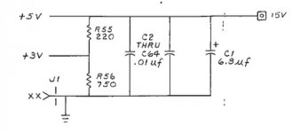
Here are my problem - based on http://www.bitsavers.org/pdf/dec/mps/docs/MPS_KC7341_EngDrwg.pdf
Any input appreciated..
Here are my problem - based on http://www.bitsavers.org/pdf/dec/mps/docs/MPS_KC7341_EngDrwg.pdf
- power.

Why is the 15v shown connected to the 5v rail? What am I misunderstanding? The resistor divider I understand (They use a lot of 3V signals on the board). They seem to use 3v rather than lots of pullups from the 5v rail for signals that are always tied high. I have not yet avo-ed the board, so I cant comment if the wee diagram is reality *it cant be* or not. - Use. Has anybody on the forum any experience of these units? I dont have a M7341 to play with, so I can only go on what the manual says.
Any input appreciated..
