intabits
Experienced Member
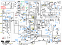
The annotated schematic for the M8650 at:-
http://tronola.com/M8650_schematic_annotated.GIF
is a pretty clear copy of the schematic, and the annotations look useful.
But the external connections to the board are all over the place in the original DEC schematic, and the annotations did not extend to those.
So I've added highlighting for the Omnibus pins, and the pins to the Berg interface connector. (and also where +/-15v is used)
My updated schematic:- (legend near bottom left corner)

Here is an "edge connector" view of the M8650 Omnibus pin usage, showing which pins are used on this board. Following that is a summary of the pins used grouped by signal type.
I'm thinking of adding a facility to my "Omnibus Browser" program to allow one to mark which pins a particular board uses, and have the program generate the listing and summary automagically.
Finally, the pinouts of the 40 pin Berg connector,the standard M8650 interface cable (which is for TTY only), and the cable I plan to make for RS232 use.
http://tronola.com/M8650_schematic_annotated.GIF
is a pretty clear copy of the schematic, and the annotations look useful.
But the external connections to the board are all over the place in the original DEC schematic, and the annotations did not extend to those.
So I've added highlighting for the Omnibus pins, and the pins to the Berg interface connector. (and also where +/-15v is used)
My updated schematic:- (legend near bottom left corner)
Here is an "edge connector" view of the M8650 Omnibus pin usage, showing which pins are used on this board. Following that is a summary of the pins used grouped by signal type.
Code:
               Omnibus Pin Checklist for Board: M8650
               (Option KL8/E Async/Serial Comms interface)

               X = Signal used    . = unused   p = Power   g=Gnd

                           Solder Side          Component Side
               Signal              Pin  X   X   Pin    Signal

               +5V                 A2A  p   X   A1A    TPA1A
               -15V                A2B  .   X   A1B    TPA1B
               GND                 A2C  g   .   A1C    SPGND
               EMA0-L              A2D  .   .   A1D    MA00-L
               EMA1-L              A2E  .   .   A1E    MA01-L
               GND                 A2F  g   g   A1F    GND
               EMA2-L              A2H  .   .   A1H    MA02-L
               MEM-START-L         A2J  .   .   A1J    MA03-L
               MD-DIR-L            A2K  .   .   A1K    MD00-L
               SOURCE-H            A2L  .   .   A1L    MD01-L
               STROBE-H            A2M  .   .   A1M    MD02-L
               GND                 A2N  g   g   A1N    GND
               INHIBIT-H           A2P  .   X   A1P    MD03-L
               RETURN-H            A2R  .   .   A1R    DATA00-L
               WRITE-L?            A2S  .   .   A1S    DATA01-L
               GND                 A2T  g   g   A1T    GND
               ROM-ADDR-L          A2U  .   .   A1U    DATA02-L
               LINK-L              A2V  .   .   A1V    DATA03-L
                                   ---          ---
               +5V                 B2A  p   X   B1A    TPB1A
               -15V                B2B  .   X   B1B    TPB1B
               GND                 B2C  g   g   B1C    GND
               INT-STROBE-H        B2D  .   .   B1D    MA04-L
               BREAK-IN-PROG-L     B2E  .   .   B1E    MA05-L
               GND                 B2F  g   g   B1F    GND
               MA,MS-LOAD-CONT-L   B2H  .   .   B1H    MA06-L
               OVERFLOW-L          B2J  .   .   B1J    MA07-L
               BREAK-DATA-CONT-L   B2K  .   X   B1K    MD04-L
               BREAK-CYCLE-L       B2L  .   X   B1L    MD05-L
               LD-ADDR-ENABLE-L    B2M  .   X   B1M    MD06-L
               GND                 B2N  g   g   B1N    GND
               INT-IN-PROG-H       B2P  .   X   B1P    MD07-L
               RES1-H              B2R  .   X   B1R    DATA04-L
               RES2-H              B2S  .   X   B1S    DATA05-L
               GND                 B2T  g   g   B1T    GND
               RUN-L               B2U  .   X   B1U    DATA06-L
               POWER-OK-H          B2V  X   X   B1V    DATA07-L
                                   ---          ---
               +5V                 C2A  p   .   C1A    TPC1A
               -15V                C2B  .   X   C1B    TPC1B
               GND                 C2C  g   g   C1C    GND
               TP1-H               C2D  .   X   C1D    I/O-PAUSE-L
               TP2-H               C2E  .   X   C1E    C0-L
               GND                 C2F  g   g   C1F    GND
               TP3-H               C2H  X   X   C1H    C1-L
               TP4-H               C2J  .   .   C1J    C2-L
               TS1-L               C2K  .   .   C1K    BUS-STROBE-L
               TS2-L               C2L  .   X   C1L    INTERNAL-I/O-L
               TS3-L               C2M  .   .   C1M    NOT-LAST-XFER-L
               GND                 C2N  g   g   C1N    GND
               TS4-L               C2P  .   X   C1P    INT-RQST-L
               LINK-DATA-L         C2R  .   X   C1R    INITIALIZE-H
               LINK-LOAD-L         C2S  .   X   C1S    SKIP-L
               GND                 C2T  g   g   C1T    GND
               IND1-L              C2U  .   .   C1U    CPMA-DISABLE-L
               IND2-L              C2V  .   .   C1V    MS,IR-DISABLE-L
                                   ---          ---
               +15V                D2A  p   X   D1A    TPD1A
               -15V                D2B  p   X   D1B    TP7
               GND                 D2C  g   g   D1C    GND
               IR0-L               D2D  .   .   D1D    MA08-L
               IR1-L               D2E  .   .   D1E    MA09-L
               GND                 D2F  g   g   D1F    GND
               IR2-L               D2H  .   .   D1H    MA10-L
               F-L                 D2J  .   .   D1J    MA11-L
               D-L                 D2K  .   X   D1K    MD08-L
               E-L                 D2L  .   X   D1L    MD09-L
               USER-MODE-L?        D2M  .   X   D1M    MD10-L
               GND                 D2N  g   g   D1N    GND
               F-SET-L             D2P  .   X   D1P    MD11-L
               PULSE-LA-H          D2R  .   X   D1R    DATA08-L
               STOP-L              D2S  .   X   D1S    DATA09-L
               GND                 D2T  g   g   D1T    GND
               KEY-CONTROL-L       D2U  .   X   D1U    DATA10-L
               SWITCH-L            D2V  .   X   D1V    DATA11-L


        M8650 Omnibus usage summary:-
        Group       Signals
        Power:      +5V, +15V, -15V, GND
        I/OData:    04-11               (but not 0-3)          (LS Byte)
        MemData:    03-11               (but not 0-2)
        TPs:        A1A, A1B, B1A, B1B, C1B, D1A, D1B
        I/OCtrl:    I/O-PAUSE-L, C0-L, C1-L
        I/OIntf:    INTERNAL-I/O-L, INT-RQST-L, SKIP-L
        MiscCtrl:   INITIALIZE-H, POWER-OK-H
        Timing2:    TP3-H
I'm thinking of adding a facility to my "Omnibus Browser" program to allow one to mark which pins a particular board uses, and have the program generate the listing and summary automagically.
Finally, the pinouts of the 40 pin Berg connector,the standard M8650 interface cable (which is for TTY only), and the cable I plan to make for RS232 use.
Code:
       J1 (Berg) connector:-
       Pin#    DEC#    Usage                   Pin#    DEC#    Usage
       1       A       Gnd                     2        B       Gnd
       3       C       Gnd                     4        D       nc
       5       E       RXDataIn (TTL)          6        F       TXD (RS232)
       7       H       Keyboard out (TTL)      8        J       RXD (RS232)
       9       K       Keyboard contact        10       L       nc
       11      M       RXDataOut (TTL)         12       N       nc
       13      P       nc                      14       R       nc
       15      S       Keyboard contact        16       T       nc
       17      U       nc                      18       V       RTS (RS232) always asserted at +6V
       19      W       nc                      20       X       nc
       21      Y       nc                      22       Z       nc
       23      AA      Printer Magnet          24       BB      nc
       25      CC      nc                      26       DD      DTR (RS232) always asserted at +6V
       27      EE      Reader relay            28       FF      nc
       29      HH      nc                      30       JJ      nc
       31      KK      Printer Magnet          32       LL      nc
       33      MM      nc                      34       NN      nc
       35      PP      Reader relay            36       RR      nc
       37      SS      nc                      38       TT      nc
       39      UU      Protective Gnd          40       VV      Signal Gnd


       KL8-E cable assembly (Part# 7008360)
       40 pin Berg connector    to              8 pin external connector
       Pin#    DEC#             colr            Pin#       Usage
       1       A                shld                       Gnd
       5       E--|             blk                        RXDDataIn (TTL)     (looped together
       7       H--|             blk                        Keyboard out (TTL)   on berg plug)
       9       K                grn             7          Keyboard contact
       15      S                red             3          Keyboard contact
       23      AA               wht             5          Printer Magnet
       27      EE               blk             4          Reader relay
       31      KK               blk             2          Printer Magnet
       35      PP               blk             6          Reader relay
       39      UU               shld


       Cable above is for 20mA TTY operation. For RS232,we need:-
       40 pin Berg connector
       Pin#    DEC#     DB9M(as DTE)     DB9F(as DCE)           Usage
       1       A        5                5                      Gnd
       5       E--|                                             RXDDataIn (TTL)  (looped together
       11      M--|                                             RXDataOut (TTL)   on berg plug)
       6       F        3                3                      TXD (RS232)
       8       J        2                2                      RXD (RS232)
       18      V        7 (RTS)          7 (CTS not neeeded)    RTS (RS232) always asserted at +6V
       26      DD       4 (DTR)          4 (DSR not neeeded)    DTR (RS232) always asserted at +6V

                        needs NM & GB    is a NM with GB        (->Use the DB9F on a cable)
                        (NM=Null Modem, GB=Gender Bender)