• Please review our updated Terms and Rules here

Microforce PLB-85 RAM expansion card in an IBM 5150

cwathen

Experienced Member
Joined
Feb 1, 2018
Messages
268
Location
Bristol, UK
Hi All,

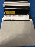
First post!. I picked up a Microforce PLB-85 multifunction card from ebay to try and expand my 5150's RAM from 256K.

The board was advertised as having an RTC, game port, 2 serial ports, parallel port and 256K of extra RAM which would bring my 5150 up to 512K

I used the parallel port to connect with Interlink on another clone with a hard drive fitted so I have got at least something out of the card.

I'm not having any luck getting the extra RAM to work though. I've set SW2 on the 5150 to 512K but boot fails with a 201 error. I did try setting it to 288K just to see if any of the RAM on the card will function, still the 201 error.

The card came with a disk but no manual. The disk has a ramdisk driver and a utility for setting the RTC. I did try setting SW2 back to 256K so the system would boot and installing the ramdisk driver for the card in case it has been set up to use the extra RAM for a ramdisk but all that did was take memory from the 256K in the 5150, not use the extra RAM on the card.

There are 3 rotary switches and several jumpers on the board, but without a manual I have no idea of knowing if they're set correctly and I can't find any information about this card online.

Hopefully someone can help!
 
Hi All,
First post!.
Welcome to these forums.

I'm not having any luck getting the extra RAM to work though. I've set SW2 on the 5150 to 512K but boot fails with a 201 error. I did try setting it to 288K just to see if any of the RAM on the card will function, still the 201 error.
I think that finding the configuration information will be very helpful, because for all you know, the RAM has been disabled by one of the switches, or the RAM has been configured for a starting address other than 256K.

But maybe it is set to start at the 256K address, but a RAM chip failure is causing the 201 error. What are the figures alongside the 201 ?

If the card's RAM chips are in sockets, a worthwhile thing to try is to re-seat the chips, in case of a poor connection.

I did try setting SW2 back to 256K so the system would boot and installing the ramdisk driver for the card in case it has been set up to use the extra RAM for a ramdisk but all that did was take memory from the 256K in the 5150, not use the extra RAM on the card.
SW2 informs the power-on self test as to how much total conventional RAM that it should find and test. So it sounds like you may not be using the correct SW2 switch settings (which vary accoring to the motherboard BIOS revision), or that you may be getting on and off confused on the switches.

Confirm that you have on/off correct per the web page at [here].

As for the correct SW2 settings, confirm that you are using the settings shown at [here], the setting for the 10/27/82 motherboard BIOS.
 
Because the OP's posts are still being moderated, the OP has PM'ed me with additional info. Addressing that via PM. Correspondence follows.

cwathen said:
If it makes any difference, I played further after my post yesterday. Booting when set to 512KB only fails totally when trying to boot from disk. With no disk, the screen will switch to 40 columns, display 'Parity 2' then will drop into BASIC and seem to function normally.
The 'Parity 2' is very informative. I presume that you meant 'PARITY CHECK 2'. The 5150 BIOS displays that when an expansion card signals a RAM parity error to the motherboard (via pin A1 per the diagram at [here].)

So there is a RAM problem on your PLB-85 card (it has encountered a parity error). The addition information that the 201 error lists will indicate the address and the bit/s, per [here].

Hopefully, just re-seating the RAM chips will fix that. Otherwise, without technical doco for the card, try swapping RAM chips about sockets, one by one, between power ons. When the address or bit indicators in the 201 error change, you know that the faulty chip is one of the two you've just swapped.

cwathen said:
Googling the particular card I've got doesn't seem to help, the only positive results I get are for the ebay listing that I've won. I don't have a manual for it (and there isn't one on the disk), there is also nothing on the card itself to say what the switches and jumpers do. The utilities on the disk are just to set a ramdisk size (which just adds a line to CONFIG.SYS for the supplied ramdisk driver and a size), to set the time and date in the RTC, and a file to add to AUTOEXEC.BAT which copies the RTC's data into the system clock at startup. There is nothing on it to read the card's configuration.
Quite standard for cards of that time.

cwathen said:
Only other thing I can think of is that the (soldered on) RTC battery is still not totally dead after all these years - it's rated at 3V but I stuck a meter on it and it is still putting out about 0.5V. I don't know if there is some pathway between the battery and the RAM and the voltage coming out is enough to cause a problem.
The RTC circuitry is completely separated from the RAM circuitry.

If the battery is a NiCad type, expect the battery to start leaking, if it hasn't already. Green stuff will start forming on nearby components, on the card and motherboard, resulting in damage.
 
The 201 error is accompanied with '4094'. From looking at minuszerodegrees, this would indicate that the problem is at 256KB, where the card is supposed to start. All of the chips on the board have been reseated, and I have swapped around the chips from bank A with those bank D to see if this would change the error, still 4094. I also tried setting the SW2 settings to 320KB to see if the card would run on just one bank. Still the same error. The 'parity check 2' error seems to be intermittent.

I did briefly think that I'd solved the problem (or I have but the board is faulty) - two of the rotary switches nearest the RAM chips are labelled from 0 to F. They were set to '8' and '0'.

So I thought 80 in hex = 128 in decimal x 4 = 512 which might mean that the board came from a system with 512KB installed and so the start address is wrong. I tried changing them to '4' and '0' (40 hex = 64 decimal x 4 = 256). Made no difference whatsoever!

It does appear these switches do control where the memory is mapped though, as if you set them both to 0 the system won't even post, not even a flashing cursor, so it appears that it is then trying to map the card into the start of RAM, and if you set them to lower numbers you can make the 201 error change to lower parts of memory.

What is supposed to happen if you map a card's start address to below the system RAM? Is the card supposed to take over those areas of RAM (in which case I can then draw the conclusion that the card is faulty) or do the two conflict which will cause failure anyway (in which case I still might have an incorrectly configured but good card).
 
Last edited:
The 201 error is accompanied with '4094'. From looking at minuszerodegrees, this would indicate that the problem is at 256KB, where the card is supposed to start.
Yes, however the "94" portion indicates three bits in error, and according to my notes, "94" is commonly seen when there is no RAM at the address. Based on that, I expect that you would see the same if you removed the card (whilst keeping the motherboard SW2 setting at something past 256K).

What is supposed to happen if you map a card's start address to below the system RAM? Is the card supposed to take over those areas of RAM ...
No. IBM put no such functionality in the design. In the PC family, overlapping RAM is a 'no no' as far as IBM is concerned.
 
Note that for the times that you think the card's switch settings are putting the RAM's starting address at something past 256K, you should be able to test for that.
Experimentation using the 'CheckIt' or 'DEBUG' methodology shown at [here] should allow you to determine the starting address.
 
Update, eventually this got sorted and was down to a large number of faulty RAM chips. The buyer generously supplied more and I am now up to 512K of RAM on my 5150. After a lot of trial and error I eventually worked out that all the RAM settings are controlled by the 3 rotary hex switches, no changes to the jumpers are needed.

Hopefully this information will be useful to someone else who gets one of these boards with no docs:

The 2 switches that are next to each other by the RAM banks set the start address. The correct settings are derived by dividing the motherboard RAM by 4 and then converting the decimal number to a 2 digit hex number which is set using the 2 switches. So for a 256K start address, you would set them to '4' and '0' (256 / 4 = 64(decimal) = 40(hex).

The third switch which is located away from the RAM banks is used to set the number of banks that you want to enable. Although it is still a hex switch labelled 0 - F, only positions 0-4 need to be used. Set it to '0' to disable the extra RAM, and then to a position from 1-4 to enable 1, 2, 3 or 4 banks respectively of RAM. I didn't investigate whether the other settings do anything else, but even if they don't they don't seem to be necessary for basic operation.

My card was originally set to 8 - 0 - 2 which would add 128K of RAM to a 512K system for 640K total, I've now got them set to 4 - 0 - 4 which adds 256K of ram to a 256K system for 512K total.

Success!
 
Back
Top