• Please review our updated Terms and Rules here

Model 4 died this morning

ldkraemer

Veteran Member
Joined
Mar 14, 2013
Messages
2,784
Location
Chaffee, MO
I was using my Model 4 this morning, and when I tried to exit mdm730 it gave me a screen of garbage.

Now, when I power it up while holding the Break Key depressed I get this screen of characters.
It never tries to boot.

P1020942.jpg

I'm hoping someone has a clue as to what to start looking for. Maybe TRS-Ian has happened to see this type problem before.
I really need to get it running ASAP, because I'm testing (TRSDOS13 & NEWDOS 80) .IPF images for Keir's disk-analyser.

Thanks.

Larry
 
That is a Model 4 Non gate array correct? I have seen that before but unfortunately never got it working again. But that was me. I hope Ian might have an answer. What rev is the motherboard? Mine was an odd Rev B. It was more like a 4p than a regular desktop version in the way of clock generation. Good luck! If need be I do have some PAL chips and a video controller chip if needed and a A,B,C ROM set too. Just let me know.
 
It could be the Z80 CPU, it seems to happen sometimes.
A bad address buffer or latch could be possible too.

I think you need a scope to monitor the activity on these lines.

Hans01
 
I would also try removing the RAM (carefully) and cleaning the pins on each chip with a white pencil eraser and re-inserting them into the sockets.

My Model III did something similar when I got it, and cleaning the legs of the RAM got it working again.
 
Frank,
My Motherboard says 1982 and has the following numbers -- 8709296 Rev C 1700219
I don't know how to tell a Non-Gate Array from the Gate Array. Is there an easy way to tell?

Al,
I've carefully removed, and reseated all IC's that are in sockets. No change other than now I get 16 of those graphic character sets across the screen and lots less
rows from what I had in the first Photo.

My Model 4 only has one Astec Power Supply, as the Floppy's I installed had a small board and powers just the two drives. I don't remember where I bought that small
Power Supply for the Drives. Originally the Model 4 was a Diskless Unit with 64K RAM. I added 64K RAM and the PAL from Tandy so I could use it with CP/M.

NF6X,
Yes, Keir has been making lots of good changes, and I've been testing lots of those changes. So far he has coded an auto Decoder that handles all CP/M Floppy's
to get the number of Sectors and Sector Size. That allows him to get the proper information for creating the .IPF from the STREAM (.RAW) preservation files.
I've tested a TRSDOS 1.3 IPF and a NewDos 80 IPF that I created with disk-analyser, and they boot and work properly. But, I don't have his lastest code
he just pushed. I will do that in the next few days.

Now I'm where I can't really do much until I get a functional Model 4.

I guess the best thing to do is verify the Astec Power Supply and then dig out my O'Scope. I was hoping it wouldn't come to that. I've got a new Z80B somewhere
but since I've moved I haven't a clue as to which box is hiding it.

I'm still hoping Ian has seen this same problem, and can point me in the right area, with the correct troubleshooting information. Otherwise it might be a long process.


Thanks.

Larry
 
Keir has also been working on some other related exciting stuff like ImageDisk (.IMD) support, RX02, and even a generic IPF creator that might work with most any format that places the write splice at the index pulse. I provided some RX02 images and tested out an IMD to IPF conversion on my model 4.

If you'll be looking at your Astec power supply anyway, it wouldn't hurt to replace any Rifa paper-dielectric caps if you haven't already. If I recall correctly, my gate array Model 4's supply had three of them in there. I replaced the ones in my Model 4 before they blew, but my Model 12 got the replacement post-smoke.
 
Just a short reply to get you started, in these instances I start by substituting all socketed chips on hand (your M4 board is a Rev C non-gate array - one of the better ones). Then I downgrade to 64K (remove U72 PAL and install a shunt (or a switch block if you don't have a shunt handy. See if the same thing happens with either bank of Ram chips.

If you are getting anything on the screen - like the pattern you are seeing - then +5V is working on the power supply. The +12V and -12V are only used on the RS232 board, and 16k ram chips. +12V is used to drive the CRT so that fact that it fires up shows the +12V supply is working. Remove the power supply and carefully inspect TB2 or just re-solder the connector even if you can't see hairline cracks.

Finally get a frequency counter and look for 2.02MHz or 4MHz on Pin 6 of the Z80, if that's missing find why the CPU clock isn't ticking.

I then start looking at address lines on the Z80 to see if any is stuck high or low and work backward from there.

Hope this gets your started...

Ian.
 
TRS-Ian,
Thanks for the starting tips.

I've figured out I need to remove the HIGH Bank of RAM U85 thru U92. Now, I have a quick question on how to set the SHUNT for U72.
The Pins for U72 are:


U72 SHUNT CONNECTIONS

NC________1___________20__+5 VDC
A16_______2___________19__*CASS2
*EXTMEM__3___________18__NC
MBIT0_____4___________17__NC
MBIT1_____5___________16__NC
FIXUPMEM_6___________15__NC
MAPON____7___________14__NC
A15_______8 ------------------ 13__MPA15
CAS_______9 ----------------- 12__*CASS1
GND______10___________11__NC

and I'm thinking I only need to connect 8 to 13, & 9 to 12. Is that what the Original SHUNT had jumpered? I can't locate my Original Shunt.
I thought I had stuck it to the bottom of my case with double sided tape.

Thanks.

Larry
 
Last edited:
Non Gate array usually had a Black White screen. And the arrow keys are left and right arrows above enter key and up down arrow keys on left side of keyboard. Also catalog number 26-1069. Gate array is catalog number 26-1069A. Shunt is a 4 pin shunt shorting the following pins: 6-15, 7-14, 8-13 & 9-12. Hope this helps.
 
Frank,
Thanks for that bit of information on the Shunt.

I've removed all RAM in U77 thru U84 (Low Bank). Moved RAM from U85 thru U92 to U77 thru 84 (High Bank to Low Bank). Removed U72 and used an IC Socket to
replace U72 with wire Jumpers from 6 to 15, 7 to 14, 8 to 13, and 9 to 12 of original IC U72.

On Power up I still have the same problem, but now I have a basic 64K system to troubleshoot. It's time to start chasing clock signals, control signals, and Address Lines.

Larry
 
Last edited:
I wish you much success! If needed let me know if you need the PAL chips. Also have the character generator chip, the Video Ram chip and the 6845 CRT controller. If needed just send me a PM. Oh and the 3 ROM chips too!
 
I'm making good prgress on the Dead Model 4. I've verified the following with my O'Scope:

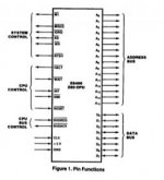
1. CPU has +5.0 VDC on Pin 11
2. CPU has Clock Signal on Pin 6

At this point it could be something STUCK on the Address Bus, Data Bus, or a defective Control Signal to CPU (INPUT to CPU).

Z80-1.jpg

The next step was to concentrate on the Control Signals that are INPUTS to the Z80 CPU. (ALL ACTIVE LOW)

1. /WAIT Pin 24 Toggles
2. /INT Pin 16 LOW ALL THE TIME
3. /NMI Pin 17 Toggles
4. /RESET Pin 26 Toggles
5. /BUSREQ Pin 25 Appears to be High all the time

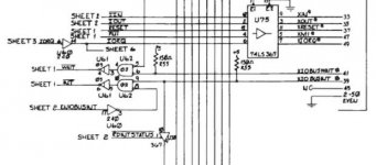
So, now I'm headed to the Circuit that generates /INT.

INT.jpg

It appears that U61 (7405) has a LOW on Pin 5 and also a LOW on Pin 6. I've removed the CPU and have the same Signal levels.
The IC U62 (74LS02) has a HIGH on Pins 8 & 9 which should produce a LOW on Pin 10.

Now, it's time to replace IC U61.


Thanks.

Larry
 
Last edited:
After removing U61 (SN7405), and locating a 14 Pin Socket, I soldered in the socket, and inserted a new SN7405. After replacing the Motherboard
in the case, I applied Power. I still had a LOW on the /INT (Pin 16) of the CPU. I thought that's impossible. But, as I searched further in the Schematics
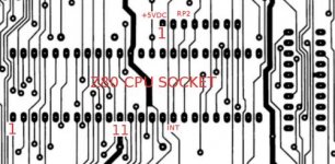
I located a SIP of PULLUP Resistors. This package is labeled RP2, is immediately above the CPU Socket, and has +5VDC applied to Pin 1, with Pins 2
thru 8 being 4.7K PULLUP Resistors.

When I used my OHM Meter to VERIFY each Resistor, each one measured 4.7K to the Common Pin (Pin 1). But, when I apply Power, the
Resistor attached to Pin 3 DOES NOT PULL the CPU Pin 16 to +5VDC (with CPU removed).

I've attached a Photo of the actual Circuit Traces (Component Side) with a few labels.

RP2-CPU.jpg

Now I've got to either Jumper a 4.7K from +5VDC to CPU Pin 16, or Order a replacement 4.7K Resistor Pack.

That should finally fix my booting problem.

I'm hoping this is the ONLY problem.

THANKS.

Larry
 
Hmm, if you measured 4.7k between the /INT net and the common pin of the resistor pack but the net isn't being pulled up, that suggests to me that the resistor pack is probably fine but something else is dragging the net down. What do you see when you measure the resistance from /INT to ground?
 
Have you tried swapping the Z80? I wonder if the CPU itself maybe pulling the /INT pin low. Pull the Z80 and measure the /INT pin and see if you get a high then. If still low than something is dragging it down!
 
NF6X,
I hate to say it buy you are correct. I double checked and the SN7405 is what is holding /INT LOW. So it's upstream. I was sure I had removed
the SN7405 and Pin 16 on the CPU didn't go HIGH, but I must have skipped that test.

So, it's back to the schematics for whatever is keeping /INT (CPU Pin 16) LOW.


Thanks for the suggestion.

Larry
 
I've got the /INT Signal on the Z80 (Pin 16) working properly now. I had the problem narrowed down to the SIP Resistor RP2,
but couldn't believe that it OHMED out at 4.7K, but didn't pull Pin 16 of the CPU "HIGH".

This morning I removed the Motherboard, and unsoldered only that Pin on the SIP RP2 and resoldered it. After replacing the Motherboard
I still didn't have a "HIGH" on /INT (Pin 16). It was being held LOW by U61 (Pin 6). As it turned out, the New Old Stock SN7405
I had inserted was defective. Luckily, I had another SN7405 and I replaced the defective one. So, now /INT is "HIGH" for the Z80.

My Clock Signal now looks like a normal clock signal. All Address Bus signals look normal too. All CPU Control Signals are now in the
correct state:
Pin 16 ___ /INT = HIGH
Pin 17 ___/NMI = HIGH
Pin 24 ___/WAIT = HIGH
Pin 25 ___/BUSREQ = HIGH
Pin 26 ___/RESET = TOGGLES "LOW" on RESET PUSHBUTTON


But, the Data Bus signals are being corrupted by something. The Data lines are more like a bunch of small Dots spread in a wavy pattern on my O'Scope.

Does anyone have a case history of likely suspect IC's that have been known to fiddle with the Data Bus and cause the Video problem
shown in the first Posting? I really don't want to replace each IC that is connected to the Data Bus.

Or, does anyone have a good method of troubleshooting Data Bus problems, when the CPU won't boot to a normal screen?


TRS-Ian, have you any clue as to a typcial cause of this problem with the Data Bus corruption? I've removed the data cable to the
Floppy Disk Controller, and that isn't it.


Thanks.

Larry
 
Last edited:
Back
Top