• Please review our updated Terms and Rules here

Most advanced BIOS that works on a IBM 5150 to support the cassette interface

Thanks for your reply, we will test your 5150 GLaBIOS on our prototype as well once we have built a prototype.

Hey Rodney,

Since we last spoke, I've decided to build IBM enhanced/extended/101 keyboard support as an option ROM. This way there is adequate code space for a full and complete implementation and it can be used with any XT BIOS you like.

Still a few weeks away from a testing release, but will let you know when it is.

640KB
 
Hi 640KB,

That is great news, thank you very much!
I do understand and appreciate how difficult your work on the GLaBIOS is because of many contraints and complexity.

Indeed using option ROMs is a good solution to have enough space to implement everything thoroughly.

I look forward to trying it out later, I know you are very busy.

Kind regards,

Rodney
 
I have thought about our 5150 type design in more detail.

I think for now it's best to at least support the original PPI ports in functionally the same manner as created by IBM since this is a standard, though short lived, of which there exist other mainboards and clones of them out there.

I will try to study some source code to find the RAM test and configuration routines. Hopefully there will be a 5150 compatible BIOS that can scan and detect the full 640KB of RAM which I will feature in hardware onboard.

I think it won't be a problem to only direct the IO space below 100h to be read from the X-BUS on our design since there are probably no mainboard ICs on the X-BUS which use higher IO ports, just the regular things. Anyway I will study the schematic in full detail as we enter it into Kicad page by page.

We will attempt to make the system support the most hardware and contain the least limitations, as long as anything we change doesn't break the 5150 functions, especially the cassette IO which is the most important issue in the project besides having normal PC functions.

As I mentioned earlier I will be looking for enhanced keyboard support to at least function so keyboard operations are comfortable and work well. Also we will be including the USB to serial mouse adapter using a RP2040 module on the mainboard as per the project by LimeProgramming.

Also I will attempt to implement turbo clock speed, which I will probably control with a normal switch or toggle circuit using a pushbutton. The PSU, power on reset and form factor etc will be ATX standard as usual in my projects so we can use a normal case and power supply to build and test the system.

The biggest issue will be BIOS support I believe.

Anyway, this project is really more and more interesting because of taking a closer look at the 5150 system which I haven't done before yet.
I am keeping an eye out for a 5150 mainboard and will buy one if I can find a good deal.
There are some odd things which look like errors in the schematic for starters which I want to confirm on the actual board.
Hopefully I can obtain the latest revision one day.

Kind regards,

Rodney
 
I don't need the parity and RAM capacity setting related pins on the PPI either, so those would be available to use as well ...
In regards to the parity related assignment, be aware that some owners, for whatever reason, may choose to run low-level hardware diagnostics. ROM based diagnostics such as Ruud's Diagnostic ROM, Supersoft/Landmark Diagnostic ROM manipulate PB4 and PB5 and examine PC6 and PC7.
 
I will try to study some source code to find the RAM test and configuration routines. Hopefully there will be a 5150 compatible BIOS that can scan and detect the full 640KB of RAM which I will feature in hardware onboard.
Per [here], only the 04/24/81 and 10/19/81 revision of IBM BIOS' do not recognise 640 KB, and that was by design. (Those BIOS' only read the first 4 switches in switch block SW2 - see [here]).

There are some odd things which look like errors in the schematic for starters which I want to confirm on the actual board.
There are definitely errors in the IBM 5150 motherboard circuit diagram. You can see some detailed at [here].
 
Hi modem7.

Thanks for your mention of this. I will probably keep the dipswitch assignment identical and I will pull the PC6 and PC7 to the non-error levels so there won't be any error thrown in diagnostics ROMs due to these inputs. I will do some testing with the ROMs you mentioned to see what will happen.

There won't normally be any need to run diagnostics since the SRAM configuration I am using will be really reliable compared to using DRAMs, but I will have a try to see what happens with those diagnostics ROMs which will be interesting to try regardless.

Kind regards,

Rodney
 
And in comparing the circuit diagrams, you will see differences. An example is the R18 shown in the diagram at [here].

And there can be other discoveries 'waiting in the wings'. For example, the text at [here] suggests a wiring problem in some 5150 motherboards.
 
Thanks for your other remarks modem7,

I checked the errors listed in your link.

I am using the schematics in the april 1984 manual.

Besides the value errors of the resistor networks and the 8288 outputs mislabeled on the nets, I also spotted another thing which to me looks odd. Maybe you can look at this?

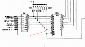
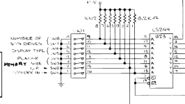
On U23 I am seeing a connection between /G1 pin 1 and the input on pin 13. That looks strange to me.
Can you confirm whether or not this is actually wired like this on a 5150?

Kind regards,

Rodney
 

Attachments

  • U23.png
    U23.png
    118.7 KB · Views: 3
I have saved some high resolution photos of the 5150 mainboard where I could check the resistor values which were missing in the schematic, such as some of the 27 ohms ones. Though those values, according to resistor function, are relatively easy to estimate regardless, just like the 4,7 ohm value which was funny to see.

The series resistors can probably be left out, I will leave the footprints in the PCB just in case there is any problem with those signals, I can check them on a scope to see what happens to the signals.

R13 on the CLK88 signal may be useful to have though. I included some 33 ohms resistors on the CLK outputs of the 8284 on my turbo XT. This also makes me consider to experiment with these to see what values result in the best signal shapes.

I will probably include some extra capacitors at the end of the ISA slots to dampen any open end reflections and crosstalk if any appears to be relatively high. One example of a potential cause of trouble is the RESETDRV on the ISA bus which is active high and thus sensitive to noise. For example UART chips don't like any noise on the RESET inputs.

I will crosscheck everything with the XT designs just to spot the changes, and consider which I should also include.
Thanks for pointing out about the resistors which warns me to look at these more carefully.

I noticed on the 5150 photos that there are very few bypass capacitors as well, which I will of course include.
Possibly they are not really needed but it's just general design practice today, at least one I am keeping myself.

Kind regards,

Rodney
 
Can you confirm whether or not this is actually wired like this on a 5150?
Give me some time to investigate.

The series resistors can probably be left out, I will leave the footprints in the PCB just in case there is any problem with those signals, I can check them on a scope to see what happens to the signals.
There are times when U14 is 'gating from B to A'. R18 put there because of the /MRDC pin of the 8288 ?

I notice that in the move to the 5160, the resistors are gone again.
 
Can you confirm whether or not this is actually wired like this on a 5150?
I didn't even bother to physically check. The circuit diagram of the 16KB-64KB motherboard shows what is expected for both motherboards. But if you really want me to, I can do a physical check.

1702247044819.png
 
Okay thank you for checking this later modem7.

During DMA cycles the CPU will be inactive, so I assume that the 8288 at those times would be aware of the inactive period and not be outputting the CPU bus control signals.

On my XT I don't have any resistors and it works fine that way.
Maybe they did it at first just to make sure in case of problems since it's more difficult if a revision would turn out to be required to add resistors later on.

Additionally, if there would exist some contention on these signals, I would expect some higher resistor value to be used and it would be poor design practice, though I have seen some creative usage of "separation resistors" for example in a ZX81, which of course is a heavily cost reduced design anyway.

Usually around 10s of ohms of resistance I would expect to be done for high frequency signals which have fast edges to dampen the feedback or current spikes on the signals possibly, or perhaps to make the waves slightly more sloped as well which might be beneficial in some situations.

I can't say for sure because I have not done some scope tests to see what happens when leaving these series resistors out. Should be interesting to check out some time when I have the chance, I will keep it in mind.

Kind regards,

Rodney
 
No problem, your image is showing what I suspect should be the actual correct circuit.
I don't really need more confirmation, thanks for the image.
 
Back
Top