gnupublic
Experienced Member
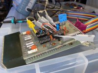
The M307A drives me crazy. I'm working on two TC08 tape controllers at a time. One is working (so lala). So I change the Flip Chips for getting the second to work also.
The second one has some defect FlipChips. One of them is the M307A, a one shot delay. This has to produce 2 delay times, one is 140ms, the other 70µs.
There are some test instructions for producing and measuring the time constants in the TC08 handbook.
With the M307B FlipChip from the first controller I get both times. But when I change to the M307A Flipchip, I don't get 140ms (70µs seems OK). I testet all parts on the board, but found nothing to be defect.
E2 9601
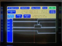
0+4 = pin 8 Output and pin 6 inverse Output
1= Input pin 1+2
2= Input pin 3
3= Input pin 4
There is the short XSTA L signal that triggers the beginning of the delay. It's going high to low during the longer positive pulse, so that the 9601 is triggered and starts the delay signal. The picture is from the working M307B.
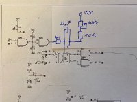
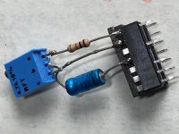
From the drawing (thanks to Vince) I tried to pull up the SN7401 (open collector E3 pin 10) with a resistor of about 1K to VCC. Then I get the 140ms delay time signal!
But this is not very stable. I think the IC's (Fairchild 9601) are OK, it seems to tell me there is a problem with the working point.
Can anybody give me a hint how to debug this?
Thanks
Volker
The second one has some defect FlipChips. One of them is the M307A, a one shot delay. This has to produce 2 delay times, one is 140ms, the other 70µs.
There are some test instructions for producing and measuring the time constants in the TC08 handbook.
With the M307B FlipChip from the first controller I get both times. But when I change to the M307A Flipchip, I don't get 140ms (70µs seems OK). I testet all parts on the board, but found nothing to be defect.

E2 9601
0+4 = pin 8 Output and pin 6 inverse Output
1= Input pin 1+2
2= Input pin 3
3= Input pin 4
There is the short XSTA L signal that triggers the beginning of the delay. It's going high to low during the longer positive pulse, so that the 9601 is triggered and starts the delay signal. The picture is from the working M307B.
From the drawing (thanks to Vince) I tried to pull up the SN7401 (open collector E3 pin 10) with a resistor of about 1K to VCC. Then I get the 140ms delay time signal!
But this is not very stable. I think the IC's (Fairchild 9601) are OK, it seems to tell me there is a problem with the working point.
Can anybody give me a hint how to debug this?
Thanks
Volker

