• Please review our updated Terms and Rules here

Powertran Cortex

The notable omission on the board is the lack of programming hardware to download the FPGA design; there is a JTAG connector but you need an external programmer device to drive it. In my case I bought I programmer (also from ebay), it works well and enables to use these low cost FPGA boards. I have a few more expensive boards which have built-in programming circuitry, but I think I prefer these cheap boards especially when messing with breadboard wiring - if the smoke decides to come out, the damage will be smaller...
OK. Diligent sell a very convenient JTAG cable as well, although somewhat more expensive than Chinese boxes: https://store.digilentinc.com/jtag-hs2-programming-cable/
It looks like this board can be piggy backed onto another PCB -- my eyes are too old to solder anything below 0.1" I think. Are those GPIO connectors on both sides, i.e. some 80 I/O pins freely available?

But to come back to this design, once I realized that level converters would not be necessary,
Are you running the system at 3.4V? Or a bit more to be stable, 3.6V or so? Does it still run at 3MHz (12MHz crystal)?

If you're interested I can post the VHDL code; although I have to say I'm not an expert on VHDL. (Getting things to work has been good enough for me... I'm much more a C++ / assembly guy, but you just cannot use those skills alone to create hardware.)
Yes, I'd be interested. Would it make sense to host the VDHL source at GitHub or so? That way there is a clear development history available for future readers. I've been thinking about learning VHDL for years but never got around to it. Perhaps 2016 will be the year.

Also I think it would be a nice exercise to implement TMS9918 functionality, and perhaps emulation, which would enable this thing to transform both into an "actual" Cortex and TI99/4A.
Actually, the mini Cortex board already has a socket for the "F18A", a custom breakout board with a Xilinx XC3 FPGA and a few level shifters, that implements a 9918 chip with VGA output. Later versions also include a 9900 core. The F18A is the brain child of Matthew Hagerty: http://codehackcreate.com/
I'm not sure it is open source, but it might be.

I also happen to have one TMS99105 chip. I'm very intrigued of the idea of hooking it directly to an FPGA, so that the address demultiplexers and memory buses could just exist inside the FPGA - there would be a lot less wiring that way.
Yup, my thinking exactly.

I think I am going to need some help to get your Unix running - although I have not yet extensively read this great thread, so I don't really have an idea on how much ground has already been covered in the messages. Anyway I want (and probably need) to get some kind of mass storage working first, and I also want to get more familiar with Stuart's port of the firmware.
Currently there is a pretty complete V6 Unix port for the mini Cortex. It could also run on a real Cortex, as long as it has been extended with a hard disk. The source code repository is here:
http://1587660.websites.xs4all.nl/cgi-bin/9995/timeline
I guess I have not documented how to get from source to a disk image, but that is easily explained once you get to it.

As a simple but hopefully useful exercise I was planning to add to Cortex basic save&load functionality to the Flash rom. The basic interpreter is a pretty handy hardware testbed.
The disk I/O routines were a later add on to Cortex Basic. We did some work on reconstructing the source code (disassembly + new comments) about one year ago; it is in this thread. Yes, from my perspective integrating this into the ROM is very useful.

Paul
 
Do you have some pointers to go to look for more info on the TI990 minis and their MMU? Well I guess I should google them up...
It is on bitsavers: http://bitsavers.informatik.uni-stuttgart.de/pdf/ti/990/

In short the TI990 MMU is a segmentation design with 3 segments. There are 3 limit registers defining the length of each segment, and 3 corresponding base registers that define the base address in physical memory for each segment. This design is repeated 3 times, once for kernel mode, once for user mode and once for LDD/LDS instructions.

In the discrete logic implementation of the TI990 CPU this is implemented with a lot of latches for the registers and a ton of comparators and adders for the logic. See the "schematics" directory at bitsavers for details.

Now that I think about it more, it may be hard to run DNOS unmodified on a 9995 chip, perhaps this is something that can only be easily done on a 99105 chip.
 
OK. Diligent sell a very convenient JTAG cable as well, although somewhat more expensive than Chinese boxes: https://store.digilentinc.com/jtag-hs2-programming-cable/
Yes, I think I actually was looking at these a while back but they were out of stock at the time. I would much rather go for one of these than any Chinese boxes. In fact I acquired an Estonian board that emulates the Xilinx cable, allowing it be used directly from Xilinx's Impact software. I live in Finland so that was close to me, it arrived in a few days. I have a Diligent board (Nexys2) and their products are solid. One thing I don't know is whether the Digilent's adept 2 software supports programming of the SPI connected flash ROM on this Spartan 6 board. The spartan 6 supports a kind of "sideband" SPI bus for boot up, and the Xilinx's impact programming suite allows one to easily program the flash and select the memory type on that SPI bus. This process is explained in the manual of the FPGA board.

It looks like this board can be piggy backed onto another PCB -- my eyes are too old to solder anything below 0.1" I think. Are those GPIO connectors on both sides, i.e. some 80 I/O pins freely available?
A good point, you are right. Indeed perhaps the best feature of the board is that those pins are readily available. It was very late when I was writing my post so I didn't mention this - I also realized that there were some words missing in my post. I guess it was still understandable. There are indeed two 40 pin connectors, making the board piggy backable. I forget the exact number of useable IO, it's probably around 72 as there are some power pins in there.

Are you running the system at 3.4V? Or a bit more to be stable, 3.6V or so? Does it still run at 3MHz (12MHz crystal)?
Yep, I am running at 3.6V and 3MHz, i.e. with 12MHz crystal. The FPGA already attempts to assert READY low before taking RESET high so zero wait states should work, but I haven't tested that yet, as I understand I may need to modify the firmware first to fix the baud rate of the UART.

Yes, I'd be interested. Would it make sense to host the VDHL source at GitHub or so? That way there is a clear development history available for future readers. I've been thinking about learning VHDL for years but never got around to it. Perhaps 2016 will be the year.
A good idea, perhaps 2016 will be the year for me to finally get something posted on github :) I'll try to set it up.

Actually, the mini Cortex board already has a socket for the "F18A", a custom breakout board with a Xilinx XC3 FPGA and a few level shifters, that implements a 9918 chip with VGA output. Later versions also include a 9900 core. The F18A is the brain child of Matthew Hagerty: http://codehackcreate.com/
I'm not sure it is open source, but it might be.
This is a very nice project, but to my understanding it is closed source. Haven't checked recently though.

Currently there is a pretty complete V6 Unix port for the mini Cortex. It could also run on a real Cortex, as long as it has been extended with a hard disk. The source code repository is here:
http://1587660.websites.xs4all.nl/cgi-bin/9995/timeline
I guess I have not documented how to get from source to a disk image, but that is easily explained once you get to it.
Thanks, I'll take a look.

The disk I/O routines were a later add on to Cortex Basic. We did some work on reconstructing the source code (disassembly + new comments) about one year ago; it is in this thread. Yes, from my perspective integrating this into the ROM is very useful.
Cool, I need to take a look at this too. It seems there is a fair bit of follow up to do. I don't know when I'll have the time for all of that, but I',m looking forward to it. Certainly you guys have done a lot of interesting stuff here!

Erik
 
In fact I acquired an Estonian board that emulates the Xilinx cable, allowing it be used directly from Xilinx's Impact software. I live in Finland so that was close to me, it arrived in a few days. I have a Diligent board (Nexys2) and their products are solid. One thing I don't know is whether the Digilent's adept 2 software supports programming of the SPI connected flash ROM on this Spartan 6 board. The spartan 6 supports a kind of "sideband" SPI bus for boot up, and the Xilinx's impact programming suite allows one to easily program the flash and select the memory type on that SPI bus. This process is explained in the manual of the FPGA board.
So what would you recommend I acquire if I want to experiment with a 99105 breadboard and an FPGA this Summer? I'm also based in the EU. (My understanding is that the 9918, the 9995 and the 99105 were all made in the same 5u NMOS process, so I think chances are that the 99105 will also run on 3.6V). The same Estonian board and the same Spartan 6 board?

Cool, I need to take a look at this too. It seems there is a fair bit of follow up to do. I don't know when I'll have the time for all of that, but I'm looking forward to it.
All of this is hobby on a 'as time permits' basis. You will note that this thread often goes silent for many months until there is something meaningful to report, so don't feel pressurized in any way.
 
So what would you recommend I acquire if I want to experiment with a 99105 breadboard and an FPGA this Summer? I'm also based in the EU. (My understanding is that the 9918, the 9995 and the 99105 were all made in the same 5u NMOS process, so I think chances are that the 99105 will also run on 3.6V). The same Estonian board and the same Spartan 6 board?

Interesting that they're all made on 5 micron process. I was earlier today wondering what might be the generational gap in terms of minimum feature size between Spartan 6 and the TMS9995.

The Estonian JTAG board does not seem to be anymore available. The eBay link to their store is http://www.ebay.com/usr/fpga.store but they seem to have very few products out there.
I think what you should get for this project with the TMS99105 are the Spartan 6 board and some reliable means of programming it, so that can focus your energy on doing something interesting instead of fighting with the setup. Probably the Diligent programming cable is a good choice.

In addition, as you are planning to learn VHDL and instantaneous gratification is normally a good thing, I would recommend that you also get an all-in-one board to test things on. This is a function of how much you are willing to spend. Although the Diligent boards are nice I would recommend either getting the Papilio Duo or the Pipistrello board. They are more affordable, have nice specs and some samples and support. I have both, but I haven't done much with the Pipistrello yet - other than using it as a logic analyzer with an additional adapter board they call "wings". The Pipistrello has a pretty sizable FPGA but is also more expensive. The Papilio Duo has the same XC6SLX9 FPGA which is on the Chinese board. I actually got started with Spartan 6 chips on the Papilio Duo, and then went for the cheap board. It might be possible to use the Papilio Duo as a programmer too for external FPGAs, at least it has a built in programming capability and easy to use software. Many of the Papilio examples are based on their ZPU based Arduino like environment. After a few quick tests I decided not to use any of that, and only used the FPGA loader program.

http://papilio.cc/index.php?n=Papilio.PapilioDUOHardwareGuide

http://saanlima.com/store/index.php?route=product/product&path=62&product_id=51

I ordered another Spartan 6 board from China, I like to have a spare one if I happen to blow up the one I am now using. If I have some time before it arrives I may end up wiring my TMS99105 to the Papilio to see what happens.

All of this is hobby on a 'as time permits' basis. You will note that this thread often goes silent for many months until there is something meaningful to report, so don't feel pressurized in any way.
Thanks for the comment, I kind of assumed as much. My intention is not to take any pressure on this, as this is supposed to be fun :)
At least for me these type of projects and my motivation go in cycles, also depending obviously on how much time there is for projects like this. Easter holidays are now over, so I don't know when I have some time and energy for this stuff. Luckily so far it has been possible to progress in small steps, getting some incremental results without investing too much time at one go.
 

Thanks for the info, I ordered another one in anticipation of some trials later.

For what it is worth, I wrote a small utility program intended for boot ROM builds, specifically for images larger than 32K. I haven't yet had the time to test it on actual chip, but it can be used to reproduce Stuart's cortex basic ROM (i.e. file compare returns identical results). I created a github repository for it: https://github.com/Speccery/packer99
There probably are still many bugs in it, I literally just got it to the point where it seems to produce meaningful results.

Next on the fun things to do is to actually modify and rebuild the ROM, with a different build ORG for the Basic to be able to page out the ROM after copying. I am also planning to put the FPGA project into github once I've cleaned it up from extra files.

Erik
 
A little bit of progress.

I had a little bit of time to work on the firmware. I got my own builds of Stuart's ROM working, and finally got to write a few lines of additional assembly code, so that I could build a new ROM. I was very happy to see that my code worked the first time around! The code is simple, but still there was a sense of achievement here as there were a bunch of loops and I am not yet very familiar with the TMS9900 assembly.
In this ROM the Basic has been compiled to address range from >2000 up to >7FFF (it actually ends at >7AB0). Thus the Basic starts code starts now from a 4K page boundary.
I wrote a little bit of code to initialize the memory paging registers, switch on paging, copying of the BASIC portion of ROM to RAM in 4K chunks i.e. page by page, and finally paging in the RAM pages to address space from >2000 to >7FFF. Only after doing this I realized that by coincidence in the ROM the addresses are exactly the same as in RAM.
Below there is a screenshot of this working (I selected option 2 after reset), including a Basic program dumping the paging registers in the FPGA. The MSB being set on the first two page registers indicates that the Flash ROM chip is enabled there. Obviously those could be copied to RAM too.
Screenshot 2016-04-02 23.27.57.jpg
 
Clearly I don't know how to properly attach screenshots so that they do not become miniaturized...
Yeah, I got stumped by that as well. It would seem that the forum squeezes images down to just a few KB and that makes screenshots unusable.

The MSB being set on the first two page registers indicates that the Flash ROM chip is enabled there.
That's an interesting approach. The original Cortex uses all bits for address space (up to 1MB of RAM), my mini-Cortex uses the high bit as a write-protect bit. The original Cortex uses the CKON and CKOF external instructions to en-/disable the MMU, I use a CRU bit for that. What do you use?

Ordered an FPGA board. Indeed, it has 72 I/O's on the GPIO connectors, plus 5V, 3V3 and GND lines. I guess I could pair it up with a strip of breadboard, use a 3.6V regulator (e.g. LM7536) to power a TMS99105 from the 5V rail and hook all CPU signal lines to the FPGA. I suppose I could use the FT232 on the FPGA board to interface with a 9902. That should be enough hardware to explore stuff like the macro instructions and the co-processor interface.

As a first step I think I should be happy to get my feet wet with VHDL and getting to operate the onboard switches and leds. Not sure I understood your earlier point about the programming cable and the SPI side channel. Would one of these be the safest choice?
 
That's an interesting approach. The original Cortex uses all bits for address space (up to 1MB of RAM), my mini-Cortex uses the high bit as a write-protect bit. The original Cortex uses the CKON and CKOF external instructions to en-/disable the MMU, I use a CRU bit for that. What do you use?
Stuart sent me the schematics of the mini-Cortex, I tried to follow that in the FPGA design, I hope I got it right. There is a flagsel register in the CRU address space at address >0140. Bit at >140 controls ROM enable and at >141 enables the MMU. I am aware from the original Cortex schematics how it handles the MAP signal generation. I had a debate with myself on what should be done here, and decided to follow the implementation of mini-Cortex. The FPGA also decodes CKON and CKOF (see source link below), although the synthesis process doesn't create them as they're not used.

I created my own firmware combo that now includes EVMBUG, BASIC and FORTH. This exceeds 32K so I needed and wanted to use the MMU to also support paging of my 256K ROM.

By the way, does anybody happen to have extra mini-Cortex PCBs I could buy? I would like to replicate the breadboard design on something a little more stable.
I really would like to start to design my own PCBs, (I have installed cadsoft eagle and played a little with it, but I haven't done anything real yet - it seems that you've used ExpressPCB, so maybe that's a better choice).

For reference, I uploaded the design to github a few days ago:
https://github.com/Speccery/fpga99
The interesting files to look at are toplevel.vhd and fpga99-xc6slx9.ucf. The latter is the user constraints file, which maps the signals to physical pins on the FPGA. The mapping there matches my pseudo random mapping on the breadboard.


Ordered an FPGA board. Indeed, it has 72 I/O's on the GPIO connectors, plus 5V, 3V3 and GND lines. I guess I could pair it up with a strip of breadboard, use a 3.6V regulator (e.g. LM7536) to power a TMS99105 from the 5V rail and hook all CPU signal lines to the FPGA. I suppose I could use the FT232 on the FPGA board to interface with a 9902. That should be enough hardware to explore stuff like the macro instructions and the co-processor interface.
If you want to follow what seems to work well on the TMS9995, you should power the TMS99105 from the 3.6V rail too or add level shifters in order not to burn the FPGA.

As a first step I think I should be happy to get my feet wet with VHDL and getting to operate the onboard switches and leds. Not sure I understood your earlier point about the programming cable and the SPI side channel. Would one of these be the safest choice?
Looking at one of the pictures it seems the components on the programmer are the same as in my programmer (I just have a PCB, no case). Probably they are based on the same design, so that should be fine. Price is reasonable too.

For getting your feet wet you can look at my design, at least there the signals are familiar so it should be easy to get going. I can also post another design for the same FPGA board to get you started without extra hardware. It is based on Jan Gray's XR16 CPU soft core and only uses the FPGA's onboard resources, plus the FTDI USB UART.
 
By the way, does anybody happen to have extra mini-Cortex PCBs I could buy? I would like to replicate the breadboard design on something a little more stable.
Yes, I have one lying around. PM me with your e-mail and we'll sort out shipping. As discussed in this thread, the PCB needs two tracks corrected to work. More troublesome is the CF Card converter board. As far as I know the last few that were floating around have all been bought. I guess if I take down my breadboard Cortex I could part with one.

I really would like to start to design my own PCBs, (I have installed cadsoft eagle and played a little with it, but I haven't done anything real yet - it seems that you've used ExpressPCB, so maybe that's a better choice).
I found ExpressPCB very easy to work with, happy to share the files.

For reference, I uploaded the design to github a few days ago
Cool.


If you want to follow what seems to work well on the TMS9995, you should power the TMS99105 from the 3.6V rail too or add level shifters in order not to burn the FPGA.
I understand that. I meant using a low-drop voltage regulator to create a 3.6V rail from the 5V rail. Now thinking that perhaps a LT3080 with a 470K variable resistor is a better choice.

Looking at one of the pictures it seems the components on the programmer are the same as in my programmer (I just have a PCB, no case). Probably they are based on the same design, so that should be fine. Price is reasonable too. For getting your feet wet you can look at my design, at least there the signals are familiar so it should be easy to get going.
Thanks. For now I'm just gathering bits and pieces. No serious hobby time until Summer. Dave Pitts is making great strides with getting more and more old Unix software to run on the 990 and I need to catch up there too.
 
Yes, I have one lying around. PM me with your e-mail and we'll sort out shipping. As discussed in this thread, the PCB needs two tracks corrected to work. More troublesome is the CF Card converter board. As far as I know the last few that were floating around have all been bought. I guess if I take down my breadboard Cortex I could part with one.
Thanks a lot Paul, that is great news! Don't worry about the CF Card converter board, I just ordered from eBay a CF to IDE connector board, I'll hack my way from there.


I found ExpressPCB very easy to work with, happy to share the files.
A big thank you again, perhaps this will finally get me started with my own boards. Has been on my to-do list for years if not decades already. I did with a friend an MC68000 board back a long time ago, nothing since then, but a LOT of manual wiring. For example I wired up by hand a TMS320C25 DSP board on an ISA bus protoboard a long time go. Worked fine with maximum clock speed, and landed me my first actual job in the industry - good memories but I think I've done my share of hand wiring... Although it is nice to be able to wire something up quickly.
 
ExpressPCB - I use it as well. It doesn't have a maximum board size like most of the other free programs seem to have. But it saves in a proprietary format so that you have to have the board made by them. Unless you buy a copy of Robot Room Copper Connection which imports ExpressPCB and exports Gerbers - it's pretty good for checking your board as well. [http://www.robotroom.com/CopperConnection/Converting-Express-PCB-Files.html]

Once you've got Gerbers, you might want to try sitopway.com for getting the boards made. Send Gerbers, quantity etc. to sales@sitopway.com and they'll normally get back to you with a quote within 24 hours or so. They take PayPal as well which is handy.

Stuart.
 
Thank Stuart! Useful information. Paul also gave me the same tips, that is good to know.

I started to put some stuff into a wiki page at github for this design.
https://github.com/Speccery/fpga99/wiki

This is somewhat off-topic, my apologies, but I wanted to quickly ask if someone has some recommendations regarding setting up a blog for this type of stuff? I have a bunch of other older hardware/software projects too that might interest someone (?), so I'd like to setup Wordpress in some hosted service. I would like to be in full control of that, so I'm not looking to jumping some of the free blog services. To say it differently, by setting up an external site it would probably force some structure and be easier for me too to organize and document some of my earlier stuff...

Erik
 
Wow - the matrix has me - I was trying to post some follow up but it said it went to admin for approval...

I was trying to say thanks to Stuart, and to say I did write some early documentation of the FPGA stuff into a wiki at github https://github.com/Speccery/fpga99/wiki

Erik
 
Some updates from my side: I've been continuing to work on the FPGA / TMS9995 breadboard when I've had some time.
The FGPA now has a working SPI controller, which has enabled me to start working on TMS9900 assembly programming to write some software to be able to work with FAT filesystem, FAT16 initially. It turns out the assembly programming is a whole lot slower than working with VHDL...

Regarding the SPI controller, I've hooked it up to a 2GB SD card, and I've gotten to a point where the code knows how to talk to the SD card, can open a partition and list its root directory, find a specific file in there, and then go through the the file while following the FAT entries (to print it, I tested a file of about 230K bytes, seems to work well). I got that working a couple of days ago, and now my plan is to build a small shell which would enable me to load programs to memory from the FAT filesystem. That should speed up software development process, burning the flash chip again all the time makes the development process slow.

Initially I found working with EVMBUG somewhat non-intuitive, but I've grown to like that old piece of code. I would want to make few improvements though, such as displaying the workspace registers when hitting a breakpoint or single-stepping. Also support for lower case would be nice too. I've continued a little the disassembly process that Stuart has done, not many more pieces of code yet disassembled but some are. It would be nice to have the entire source, to be able relocate the code and freely modify it. For the FAT code it has been nice to be able to run it from RAM, and do quick patches with EVMBUG to fix bugs.

The SPI controller VHDL code is now on the github site (it's embedded in the other VHDL code). Just out of interest I also synthesized just the SPI portion for an Altera CPLD (EPM3064 - this is 5V tolerant and has PLCC44 package, so it could be easily added to any board), as I was thinking the SPI controller might be interesting to others. The synthesis result did not occupy the whole CPLD, so there would be space for some other stuff too. In the FPGA implementation the SPI port runs currently at 6.25MHz, which pretty much means that it always transfers a byte of data before the CPU has time to access it again. It would be easy to run it even faster, or slower for that matter.

Another thing I really would want to improve is to add support for interrupts from the UART within the firmware. I think I read from somewhere that the TMS9902 can create spurious interrupts, so I am wondering if you guys have some experience with it? It would be nice to have a proper receive buffer, to stop losing characters. An alternative is to put another UART into the FPGA itself, I've used a design which has a 8 or 16 byte hardware receive FIFO. It could be interesting to implement a TMS9902 register compatible UART in the FPGA. Another option would be to setup the built-in timer of the TMS9995 and poll the UART from a timer interrupt routine.

Erik
 
Some updates from my side: I've been continuing to work on the FPGA / TMS9995 breadboard when I've had some time.
The FGPA now has a working SPI controller, which has enabled me to start working on TMS9900 assembly programming to write some software to be able to work with FAT filesystem, FAT16 initially.
That is great progress!

Regarding the SPI controller, I've hooked it up to a 2GB SD card, and I've gotten to a point where the code knows how to talk to the SD card, can open a partition and list its root directory, find a specific file in there, and then go through the the file while following the FAT entries (to print it, I tested a file of about 230K bytes, seems to work well).
2GB/FAT16 would seem to be a good choice. Note that according to the SD spec larger cards must use FAT32. One issue I had with CF cards is that some are formatted with a Volume Boot Record (= a partition table) in the first sector, and others start with a Partition Boot Record (= the PBP etc.). Does that happen with SD cards as well? (flash USB disks seem to be the same as CF cards). I've only found one vague reference on how to tell the two forms apart: apparently old IBM boot roms would look at the first nine bytes and if all are zero it is a Volume Boot Record.

I got that working a couple of days ago, and now my plan is to build a small shell which would enable me to load programs to memory from the FAT filesystem. That should speed up software development process, burning the flash chip again all the time makes the development process slow.
Yes. My own plan was that the flash chip would have code that looked at /boot on the card and would build a boot menu from the items found there. It would then load and run the selected item. However, I have no working code for that and ideas are a dime a dozen.

Initially I found working with EVMBUG somewhat non-intuitive, but I've grown to like that old piece of code. I would want to make few improvements though, such as displaying the workspace registers when hitting a breakpoint or single-stepping. Also support for lower case would be nice too. I've continued a little the disassembly process that Stuart has done, not many more pieces of code yet disassembled but some are. It would be nice to have the entire source, to be able relocate the code and freely modify it. For the FAT code it has been nice to be able to run it from RAM, and do quick patches with EVMBUG to fix bugs.
Having line editing and even better a simple history feature would be great as well. Have you seen this document from Stuart:
ftp://bitsavers.informatik.uni-stuttgart.de/pdf/ti/TMS9900/tm990-100/MP324_990-401_TIBUGlst.pdf
It is not EVMBUG, but the code is closely related to it.

Another thing I really would want to improve is to add support for interrupts from the UART within the firmware. I think I read from somewhere that the TMS9902 can create spurious interrupts, so I am wondering if you guys have some experience with it? It would be nice to have a proper receive buffer, to stop losing characters.
Not sure I have noticed this. The 9902 has multiple interrupt sources and the service routine must check the status register to find out which source(s) triggered the current interrupt. I think it is hard to overrun EVMBUG, but easy to overrun Cortex Basic. I have solved that by adding a small character delay when sending Cortex Basic source code to the breadboard.

Paul
 
That is great progress!
Thanks Paul!

2GB/FAT16 would seem to be a good choice. Note that according to the SD spec larger cards must use FAT32. One issue I had with CF cards is that some are formatted with a Volume Boot Record (= a partition table) in the first sector, and others start with a Partition Boot Record (= the PBP etc.). Does that happen with SD cards as well? (flash USB disks seem to be the same as CF cards). I've only found one vague reference on how to tell the two forms apart: apparently old IBM boot roms would look at the first nine bytes and if all are zero it is a Volume Boot Record.
The card I am currently using does have a normal MBR, my code just goes through the 4 entries looking for a FAT16 partition and goes there. From sources in the net it seems some SD cards do not have normal formatting, they just start off with the boot sector. I suppose that could be detected by looking for a x86 jump instruction in the beginning of the sector. I'm also planning to add support for FAT32, it seems there are only a few changes necessary to minimally support FAT32. SDHC support would also be needed there. I have to investigate more, but it seems SDHC only requires the code to treat 32-bit addresses as sector numbers instead of sector aligned absolute addresses on the card - my code already does this, it just upshifts the sector numbers by 9 before issuing that to the card.

Yes. My own plan was that the flash chip would have code that looked at /boot on the card and would build a boot menu from the items found there. It would then load and run the selected item. However, I have no working code for that and ideas are a dime a dozen.
That is a nice idea!

Having line editing and even better a simple history feature would be great as well.
Thinking about command history is how I discovered the character loosing issue: as an example, pressing the up key sends 3 characters (ESC [ A). The middle one is lost while the test code snippet was HEX printing the first one. EVMBUG primarily looses characters when it is printing stuff in a busy loop. Actually a simple way to fix this would be to have the XOP 12 also check for incoming characters and buffer them for later, that would work without interrupts.

Have you seen this document from Stuart:
ftp://bitsavers.informatik.uni-stuttgart.de/pdf/ti/TMS9900/tm990-100/MP324_990-401_TIBUGlst.pdf
It is not EVMBUG, but the code is closely related to it.
No I haven't, thanks!

Not sure I have noticed this. The 9902 has multiple interrupt sources and the service routine must check the status register to find out which source(s) triggered the current interrupt. I think it is hard to overrun EVMBUG, but easy to overrun Cortex Basic. I have solved that by adding a small character delay when sending Cortex Basic source code to the breadboard.
I was initially testing the SPI controller with FORTH, editing on my Mac or PC and copying the code over. Really long line delays were necessary in order not to loose characters. Thinking this a bit more, a receive buffer would not help (unless it was very large) since at least FORTH not only echoes back the characters but also prints "ok"s at the end of each line, so in addition to processing delay it adds more stuff to send to the host. I was also thinking about making an XMODEM receiver to solve that, but I suppose when it can boot from the SD card, things are solved.

I was also thinking for debugging purposes to create a modified simulator, that would run on the host but pass all I/O commands (CRU and memory mapped I/O) over the serial line to the actual hardware for execution. Would be nice for filesystem code debugging.

Erik
 
Paul,
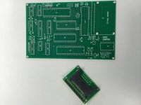
I was able to pick up the mini cortex PCB from the post office today. Thank you very much for sending it!

Erik
IMG_4632.jpg
 
Back
Top