- VCF South West - June 14 - 16, Davidson-Gundy Alumni Center at University of Texas at Dallas
- VCF West - Aug 2 - 3, Computer History Museum, Mountain View, CA
- VCF Midwest - Sept 7 - 8 2024, Schaumburg, IL
- VCF SoCal - Mid February 2025, Location TBD, Southern CA
- VCF East - April 2025, Infoage Museum, Wall NJ
-
Please review our updated Terms and Rules here
- Forums
- Companies
- IBM Computers, PCs, Clones and Descendants
- PCs and Clones (XT and early AT class machines)
You are using an out of date browser. It may not display this or other websites correctly.
You should upgrade or use an alternative browser.
You should upgrade or use an alternative browser.
Project to create an ATX 80286 mainboard based on the IBM 5170
- Thread starter rodney
- Start date
Indeed, I will test other BIOS versions yet. I will add it to my list.
However the MR BIOS is the one BIOS in which I have the most faith.
There are of course others, thanks Alvaro for the URL I will check it out.
Today I tested with power-on reset enabled in the CPLDs and with disabling race condition prevention measures.
All yielded no change or improvement.
I will test more with different latches and transceivers as well.
I want to replace some of them to see if the wave shapes will improve.
I keep getting a feeling that the CPU is either not functioning reliably at power-on or possibly some signal on the transceivers is missing the right timing.
Why this would be variable at each power cycle remains unknown and is an important issue as well.
Hak Foo thanks for your input. I have the mainboard, VGA card, harddisk, floppy disk and sound card in the system.
The power supply appears to be okay and the power rails are stable and reasonable voltages.
I did some testing and generated about one amp of current on 12V
This pulls the 5V rail exactly on 5.00V
Good call that this is happening Hak Foo.
It didn't have any effect on the problems but was good to at least look at.
The reset button has varied effects. Sometimes during an error condition where I see the data bits active but no good start of the PC, after a reset the data bits can become inactive after reset clears.
Or the state of the data bits and the erroneous pattern returns after the reset.
Sometimes the data bits stop activity after a few resets.
If the system comes up properly during one of those more rare power cycles where the system works, reset can be applied as often as I want and it always returns a working system so the reset works properly in that case.
I found the cause of the missing coprocessor problem stopping the CPU when it is executing without a coprocessor.
It turned out that the /ERROR line became active inside the IO decoder CPLD due to undefined logic state or logic 0 which caused an IRQ13 to happen.
The CPU then responds to this under certain conditions which is after a short period, and waits for the coprocessor error to be reset.
So I removed the coprocessor and added a 1k pullup resistor to /ERROR which solved that problem where the system stopped at CPU and memory detection by the MR BIOS.
Now I also can control the system without a coprocessor present.
So the pull up on /ERROR is the solution for now for that issue which was the first problem I encountered when doing tests of the system.
The coprocessor ERROR handling needs further testing but for now I ignore this for the sake of handling other issues first.
I will examine this issue and revisit the logic for U130 analysed by Johann if necessary.
I would need to have a ERROR happening in the coprocessor to see if the system deals with it.
But that's something possibly for later.
So now I first want to look at the power on situation what the cause is of the many different CPU data bit conditions happening, needing all these power cycles to get the system up.
Which is the most problematic issue at the moment.
I will upload some scope screens later which show the different patterns I am seeing.
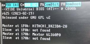
I have made a new XT-IDE AT configuration and tested with the primary and secondary IDE ports.
It appears to work properly now.
I can see a harddisk attached to the secondary, and I can see partition information in FDISK.
I tested with a NTFS drive but I will format one later on.
It seems that the MR BIOS is having some trouble with the configuration where there is only a drive attached to the secondary IDE port.
But I think it's fine when having a drive on both IDE ports.
So that's just a side note. I will do more testing later and test a CDROM drive etc.
But first I continue with sorting out the other main issues.
Attachments
I have done a lot of testing, and expanded my list of things to look at. Last night I was even unable to get the CPU to run properly anymore.
I am retracing my steps and restoring the initial situation. I can't exclude that there may be some marginal problem in one of the CPLDs even since they are recycled chips. Also I will do more work to test all the ICs once more to make sure no ICs are defective. I need to make sure of a lot of things since I can't get any normal POST and CPU operation going right now.
If someone is reading this thread who knows about the operation of Quartus in compiling a CPLD design, what I still am not sure of is the output pin operation when we want a bidirectional function. Like for example XA0 and XBHE. They are always inputs and controlled by the CPU, except those times when the AT is doing DMA operations, which will have the CPU in hold status and the A0 and BHE are floating. So in certain situations when there is a DMA operation the CPLD will need to generate XA0 and XBHE to control the high and low byte transceivers during the operations, including when there is high to low byte conversion needed. So in all situations the XA0 and XBHE should not be an output, except when it is necessary for DMA operations. So I wired these lines to the proper circuits for decoding their states, and connected a "TRI" element to these pins to control them during the DMA operations. The conditions are known and fed into the tri state control pins of these TRI elements. And I entered the pins XA0 and XBHE as "bidirectional" type pins in the quartus design. So in theory it should be right, but it's hard to actually confirm the tri state operation since I can't know how quartus deals with this. This information I could not find anywhere which confirms that type of pin operation. The documentation focuses more on the complex type of CPLD programming like bus operations, ALU type functions etc.
What's also strange and unclear is the fact that quartus appears to assign a "open drain" type of pin configuration to XA0, but not to XBHE. The open drain type of output mode would suggest that there would be a pull-up resistor needed in that case. So why we have this at XA0 and not at XBHE. I looked everywhere but it seems that the user cannot define this but rather at compile time this is determined by quartus itself. When opening the "Technology Map Viewer" this can be observed when looking at both these bidirectional pins. There is no setting to be found anywhere, and I didn't define any either. Weird stuff. And of course I need to convert the design from POF to JED where we have another setting for "open collector" which I left at "auto" in the hope that this can identify the pins which need it and apply the correct output pin programming in the JED file.
Any situation where you have more than one open variables will reach a level of complexity which makes it harder to identify problems and issues. So as discussed I tried to prevent and exclude what I can before hand and even during the test work, but now at the test phase there are always in my experience some practical issues introduced which cannot be see when purely looking at schematics. So when errors occur, I try to make very sure of as many factors as possible, that's the only way to approach the matter since I don't have advanced equipment which allow me to analyse multiple signals simultaneously. In fact I have no professional equipment to speak of so the process is made more difficult by this fact. If all fails I may slow down the clock pulse considerably and see if I can identify problems in that way. But first I prefer to look at the system under normal intended operation since that is what I usually do when debugging prototypes. This AT is much more complex to deal with than 8 bit systems and it is definitely showing up a lot in the work I am doing these days.
Right now I am working to restore everything to the initial known functional test situation and after I can confirm functionality I can proceed again with testing and debugging from there. But first now I need to retrace.
What I also want to mention is that I am suspecting one of the reasons for the random power up situations is that possibly certain clock signals need to be running in synchronized state. This is also why I modified the DMA clock frequency to 4Mhz for the time being, just in case the BIOS is doing something with the DMA controllers which needs to happen in sync in order to pass the POST operations and checks. So I am matching the DMA clock to the original 5170 4Mhz frequency and circuits later. But for now I am first restoring the original programming of the CPLDs to attempt to get the CPU operational. This is made more difficult by the fact that I need at least 20-40 power cycles before I get a working state of the CPU and system.
Last edited:
I went back to the initial programming of the CPLDs and restored the ICs used in the initial testing.
After doing this I was able to get the system to POST again.
I started a debugging log where I am logging every change and then do some power cycle tests to record how many cycles are needed after each modification.
When a change appears to provide some improvement, I keep the change in place. This better allows to trace back any changes in case of problems.
I have started to exchange a few transceivers with other logic family ones to see if this helps. If the number of power cycles needed decreases that would indicate an improvement. I will also test with the CPLD logic to see if anything can be gained from changing these. Maybe I should convert the programming logic to VHDL or similar to see if I can make subtle changes like changing the timings.
I discovered a few more things. The timer chip as far as I know normally should output a pulse of around 18Hz on output 0 continuously, however it stops doing that during the boot process when looking for a boot disk, which is not good. I replaced the timer chip and I found that the timing pulse remained a little longer but after a few reboots and the BIOS looking for a boot disk, the timer again stopped pulsing on output 0.
I checked the IO control method by IBM once more, the IO port is decoded from the address lines and /ACK only, and then chip-enables the timer which if selected then can be programmed by IO access which triggers /XIOR and /XIOW, which when combined then allows access to the timer via IO ports 040-043.
Something strange is going on where the timer stops pulsing the system timer pulse around the time when the BIOS attempts to boot.
I wonder what can happen to stop the timer which I think is not correct. Also the timer chips (Intel ones) become rather hot.
I may test by adding more detailed decoding to the timer. I mean, I know it's not supposed to be stopped by anything but if I can prevent that from happening in whatever way, I could at least test the difference to see how the system functions if the timer keeps running on channel 0 to trigger IRQ0 at 18Hz.
I also studied the Copam PC-501 schematics in more detail lately and I found several things, one of these being that they replaced the 74LS646 by a clocked latch and transceiver. They decoded the signals with a PAL and a 139 decoder to select one or the other. I also noticed that the data clocking is done in the other direction compared to what IBM did. After I get this prototype to work properly I will also look into this principle to see if I can deduce how they have done this. From the signal names etc I think I may be able to piece this together, I can test it on the prototype. I would prefer to use some more readily available standard TTL parts than the 74LS646. This would also allow to choose latches and transceivers from other logic families such as HCT or ALS etc.