| VCF West | Aug 01 - 02 2025, | CHM, Mountain View, CA |
| VCF Midwest | Sep 13 - 14 2025, | Schaumburg, IL |
| VCF Montreal | Jan 24 - 25, 2026, | RMC Saint Jean, Montreal, Canada |
| VCF SoCal | Feb 14 - 15, 2026, | Hotel Fera, Orange CA |
| VCF Southwest | May 29 - 31, 2026, | Westin Dallas Fort Worth Airport |
| VCF Southeast | June, 2026 | Atlanta, GA |
-
Please review our updated Terms and Rules here
- Forums
- Companies
- IBM Computers, PCs, Clones and Descendants
- PCs and Clones (XT and early AT class machines)
You are using an out of date browser. It may not display this or other websites correctly.
You should upgrade or use an alternative browser.
You should upgrade or use an alternative browser.
Project to create an ATX 80286 mainboard based on the IBM 5170
- Thread starter rodney
- Start date
Indeed, I will test other BIOS versions yet. I will add it to my list.
However the MR BIOS is the one BIOS in which I have the most faith.
There are of course others, thanks Alvaro for the URL I will check it out.
Today I tested with power-on reset enabled in the CPLDs and with disabling race condition prevention measures.
All yielded no change or improvement.
I will test more with different latches and transceivers as well.
I want to replace some of them to see if the wave shapes will improve.
I keep getting a feeling that the CPU is either not functioning reliably at power-on or possibly some signal on the transceivers is missing the right timing.
Why this would be variable at each power cycle remains unknown and is an important issue as well.
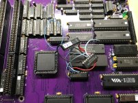
Hak Foo thanks for your input. I have the mainboard, VGA card, harddisk, floppy disk and sound card in the system.
The power supply appears to be okay and the power rails are stable and reasonable voltages.
I did some testing and generated about one amp of current on 12V
This pulls the 5V rail exactly on 5.00V
Good call that this is happening Hak Foo.
It didn't have any effect on the problems but was good to at least look at.
The reset button has varied effects. Sometimes during an error condition where I see the data bits active but no good start of the PC, after a reset the data bits can become inactive after reset clears.
Or the state of the data bits and the erroneous pattern returns after the reset.
Sometimes the data bits stop activity after a few resets.
If the system comes up properly during one of those more rare power cycles where the system works, reset can be applied as often as I want and it always returns a working system so the reset works properly in that case.
I found the cause of the missing coprocessor problem stopping the CPU when it is executing without a coprocessor.
It turned out that the /ERROR line became active inside the IO decoder CPLD due to undefined logic state or logic 0 which caused an IRQ13 to happen.
The CPU then responds to this under certain conditions which is after a short period, and waits for the coprocessor error to be reset.
So I removed the coprocessor and added a 1k pullup resistor to /ERROR which solved that problem where the system stopped at CPU and memory detection by the MR BIOS.
Now I also can control the system without a coprocessor present.
So the pull up on /ERROR is the solution for now for that issue which was the first problem I encountered when doing tests of the system.
The coprocessor ERROR handling needs further testing but for now I ignore this for the sake of handling other issues first.
I will examine this issue and revisit the logic for U130 analysed by Johann if necessary.
I would need to have a ERROR happening in the coprocessor to see if the system deals with it.
But that's something possibly for later.
So now I first want to look at the power on situation what the cause is of the many different CPU data bit conditions happening, needing all these power cycles to get the system up.
Which is the most problematic issue at the moment.
I will upload some scope screens later which show the different patterns I am seeing.
However the MR BIOS is the one BIOS in which I have the most faith.
There are of course others, thanks Alvaro for the URL I will check it out.
Today I tested with power-on reset enabled in the CPLDs and with disabling race condition prevention measures.
All yielded no change or improvement.
I will test more with different latches and transceivers as well.
I want to replace some of them to see if the wave shapes will improve.
I keep getting a feeling that the CPU is either not functioning reliably at power-on or possibly some signal on the transceivers is missing the right timing.
Why this would be variable at each power cycle remains unknown and is an important issue as well.
Hak Foo thanks for your input. I have the mainboard, VGA card, harddisk, floppy disk and sound card in the system.
The power supply appears to be okay and the power rails are stable and reasonable voltages.
I did some testing and generated about one amp of current on 12V
This pulls the 5V rail exactly on 5.00V
Good call that this is happening Hak Foo.
It didn't have any effect on the problems but was good to at least look at.
The reset button has varied effects. Sometimes during an error condition where I see the data bits active but no good start of the PC, after a reset the data bits can become inactive after reset clears.
Or the state of the data bits and the erroneous pattern returns after the reset.
Sometimes the data bits stop activity after a few resets.
If the system comes up properly during one of those more rare power cycles where the system works, reset can be applied as often as I want and it always returns a working system so the reset works properly in that case.
I found the cause of the missing coprocessor problem stopping the CPU when it is executing without a coprocessor.
It turned out that the /ERROR line became active inside the IO decoder CPLD due to undefined logic state or logic 0 which caused an IRQ13 to happen.
The CPU then responds to this under certain conditions which is after a short period, and waits for the coprocessor error to be reset.
So I removed the coprocessor and added a 1k pullup resistor to /ERROR which solved that problem where the system stopped at CPU and memory detection by the MR BIOS.
Now I also can control the system without a coprocessor present.
So the pull up on /ERROR is the solution for now for that issue which was the first problem I encountered when doing tests of the system.
The coprocessor ERROR handling needs further testing but for now I ignore this for the sake of handling other issues first.
I will examine this issue and revisit the logic for U130 analysed by Johann if necessary.
I would need to have a ERROR happening in the coprocessor to see if the system deals with it.
But that's something possibly for later.
So now I first want to look at the power on situation what the cause is of the many different CPU data bit conditions happening, needing all these power cycles to get the system up.
Which is the most problematic issue at the moment.
I will upload some scope screens later which show the different patterns I am seeing.
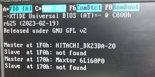
I have made a new XT-IDE AT configuration and tested with the primary and secondary IDE ports.
It appears to work properly now.
I can see a harddisk attached to the secondary, and I can see partition information in FDISK.
I tested with a NTFS drive but I will format one later on.
It seems that the MR BIOS is having some trouble with the configuration where there is only a drive attached to the secondary IDE port.
But I think it's fine when having a drive on both IDE ports.
So that's just a side note. I will do more testing later and test a CDROM drive etc.
But first I continue with sorting out the other main issues.
Attachments
I have done a lot of testing, and expanded my list of things to look at. Last night I was even unable to get the CPU to run properly anymore.
I am retracing my steps and restoring the initial situation. I can't exclude that there may be some marginal problem in one of the CPLDs even since they are recycled chips. Also I will do more work to test all the ICs once more to make sure no ICs are defective. I need to make sure of a lot of things since I can't get any normal POST and CPU operation going right now.
If someone is reading this thread who knows about the operation of Quartus in compiling a CPLD design, what I still am not sure of is the output pin operation when we want a bidirectional function. Like for example XA0 and XBHE. They are always inputs and controlled by the CPU, except those times when the AT is doing DMA operations, which will have the CPU in hold status and the A0 and BHE are floating. So in certain situations when there is a DMA operation the CPLD will need to generate XA0 and XBHE to control the high and low byte transceivers during the operations, including when there is high to low byte conversion needed. So in all situations the XA0 and XBHE should not be an output, except when it is necessary for DMA operations. So I wired these lines to the proper circuits for decoding their states, and connected a "TRI" element to these pins to control them during the DMA operations. The conditions are known and fed into the tri state control pins of these TRI elements. And I entered the pins XA0 and XBHE as "bidirectional" type pins in the quartus design. So in theory it should be right, but it's hard to actually confirm the tri state operation since I can't know how quartus deals with this. This information I could not find anywhere which confirms that type of pin operation. The documentation focuses more on the complex type of CPLD programming like bus operations, ALU type functions etc.
What's also strange and unclear is the fact that quartus appears to assign a "open drain" type of pin configuration to XA0, but not to XBHE. The open drain type of output mode would suggest that there would be a pull-up resistor needed in that case. So why we have this at XA0 and not at XBHE. I looked everywhere but it seems that the user cannot define this but rather at compile time this is determined by quartus itself. When opening the "Technology Map Viewer" this can be observed when looking at both these bidirectional pins. There is no setting to be found anywhere, and I didn't define any either. Weird stuff. And of course I need to convert the design from POF to JED where we have another setting for "open collector" which I left at "auto" in the hope that this can identify the pins which need it and apply the correct output pin programming in the JED file.
Any situation where you have more than one open variables will reach a level of complexity which makes it harder to identify problems and issues. So as discussed I tried to prevent and exclude what I can before hand and even during the test work, but now at the test phase there are always in my experience some practical issues introduced which cannot be see when purely looking at schematics. So when errors occur, I try to make very sure of as many factors as possible, that's the only way to approach the matter since I don't have advanced equipment which allow me to analyse multiple signals simultaneously. In fact I have no professional equipment to speak of so the process is made more difficult by this fact. If all fails I may slow down the clock pulse considerably and see if I can identify problems in that way. But first I prefer to look at the system under normal intended operation since that is what I usually do when debugging prototypes. This AT is much more complex to deal with than 8 bit systems and it is definitely showing up a lot in the work I am doing these days.
Right now I am working to restore everything to the initial known functional test situation and after I can confirm functionality I can proceed again with testing and debugging from there. But first now I need to retrace.
What I also want to mention is that I am suspecting one of the reasons for the random power up situations is that possibly certain clock signals need to be running in synchronized state. This is also why I modified the DMA clock frequency to 4Mhz for the time being, just in case the BIOS is doing something with the DMA controllers which needs to happen in sync in order to pass the POST operations and checks. So I am matching the DMA clock to the original 5170 4Mhz frequency and circuits later. But for now I am first restoring the original programming of the CPLDs to attempt to get the CPU operational. This is made more difficult by the fact that I need at least 20-40 power cycles before I get a working state of the CPU and system.
Last edited:
I went back to the initial programming of the CPLDs and restored the ICs used in the initial testing.
After doing this I was able to get the system to POST again.
I started a debugging log where I am logging every change and then do some power cycle tests to record how many cycles are needed after each modification.
When a change appears to provide some improvement, I keep the change in place. This better allows to trace back any changes in case of problems.
I have started to exchange a few transceivers with other logic family ones to see if this helps. If the number of power cycles needed decreases that would indicate an improvement. I will also test with the CPLD logic to see if anything can be gained from changing these. Maybe I should convert the programming logic to VHDL or similar to see if I can make subtle changes like changing the timings.
I discovered a few more things. The timer chip as far as I know normally should output a pulse of around 18Hz on output 0 continuously, however it stops doing that during the boot process when looking for a boot disk, which is not good. I replaced the timer chip and I found that the timing pulse remained a little longer but after a few reboots and the BIOS looking for a boot disk, the timer again stopped pulsing on output 0.
I checked the IO control method by IBM once more, the IO port is decoded from the address lines and /ACK only, and then chip-enables the timer which if selected then can be programmed by IO access which triggers /XIOR and /XIOW, which when combined then allows access to the timer via IO ports 040-043.
Something strange is going on where the timer stops pulsing the system timer pulse around the time when the BIOS attempts to boot.
I wonder what can happen to stop the timer which I think is not correct. Also the timer chips (Intel ones) become rather hot.
I may test by adding more detailed decoding to the timer. I mean, I know it's not supposed to be stopped by anything but if I can prevent that from happening in whatever way, I could at least test the difference to see how the system functions if the timer keeps running on channel 0 to trigger IRQ0 at 18Hz.
I also studied the Copam PC-501 schematics in more detail lately and I found several things, one of these being that they replaced the 74LS646 by a clocked latch and transceiver. They decoded the signals with a PAL and a 139 decoder to select one or the other. I also noticed that the data clocking is done in the other direction compared to what IBM did. After I get this prototype to work properly I will also look into this principle to see if I can deduce how they have done this. From the signal names etc I think I may be able to piece this together, I can test it on the prototype. I would prefer to use some more readily available standard TTL parts than the 74LS646. This would also allow to choose latches and transceivers from other logic families such as HCT or ALS etc.
I have tested a lot of different combinations of transceivers, this resulted in a reasonably optimal setup as far as the transceivers can influence the system.
Next I had a good look at various options in quartus. From my testing work I am starting to see the problem is related to timing in the CPLDs being too fast.
This just cannot be an equivalent of TTL ICs as done in the 5170, which is the problem I am sure, since everything else is a functional match with the 5170 in areas where it matters.
I have found some options in quartus which allow to disable the open drain option I was seeing at one output.
So this is now fixed to become a normal bidirectional output pin as I originally wanted to do.
I believe that the system controller CPLD is the most critical part in terms of being more timing sensitive than the other CPLDs.
I changed some options to attempt to slow down the system controller. Additionally I used a 15ns part instead of 10ns in order to get somewhat slower timing.
I was able to compile a working version of the system controller. From the tests I can see that this slightly improves the situation:
- now I need around 10 power cycles to get the CPU to power up in a functional state
- now I can start the DOS editor normally which I couldn't before
- generally there are less corruptions on the screen characters
The problem with the timer stopping to function at the moment of seeking a boot device is not solved yet.
I will focus more on the IO decoder to see if this timer problem can be fixed.
If anyone reads this post/thread and knows how I can introduce slower timing in the quartus design please let me know about some possible methods.
I think the standard method would be to introduce a very fast global clock signal and creating some kind of design restraint file which at compile time can change the CPLD program file to produce the slower output signals.
On the other hand, there must be some method to manually create some delays in a CPLD.
I will continue to do research about this.
I believe the only solution to the problems is by delaying certain logic inside the CPLDs.
If anyone has some tips how this can be done I would appreciate it if you can share it here.
Otherwise I will share my own findings here so anyone looking for this information at least can find the things I have found to be helpful.
I tried to convert the design file to VHDL however I will need to rename a lot of signals since they throw an error that these are not VHDL compatible.
I will be converting the whole system controller design and try to convert it to VHDL.
I hope I can find some clues about how to delay and slow down signals in VHDL for a CPLD.
In the past when I was designing pure TTL systems it was easier to influence the timing. Or at least, I had a direct means to change the timing. What I did with those systems was to exchange the logic family of ICs in the decoders. By changing them to faster types, I could shorten the propagation time, and by exchanging certain ICs with slower types, I could delay the propagation times. This was in certain areas especially a big influence and could even change the timing so much that the whole system would not be able to even come up with a display or ROM/RAM activity. So far I have designed and built around 5 system mainboards and I have always been able to fine tune the system so the timing is sufficient in all areas.
Recently after working on the 5170 based AT design, I discovered the ALS logic family, and at least, I have now a small supply of chips which I can harvest from the two out of four mainboards which are unstable and function poorly. So I was able to further speed up the logic on my revision 3 XT PC which made a much larger selection of DMA controller ICs work 100% with that system.
Same goes for the 8-bit XT-IDE. Many people have trouble with the XT-IDE. However what many don't realize is that they can fix the problem by changing the timing on the PCB. The high to low byte and low to high byte translations to communicate with the 16 bit drive needs to have very narrow timing to catch the correct data from the bus or present the data to the drive on time.
It's lucky that with the design of this project, as it is, we can at least achieve a POST and initialize the VGA display. This allows further experimentation and doing work to reach the phase of seeing improvements in the areas which show timing related symptoms.
I believe the main problems will be located in the system controller CPLD which generates a lot of control outputs for the system which are the most sensitive to timing.
Unfortunately, we can't change any timing in the quartus schematic diagram in similar ways as I was doing in the previous TTL logic mainboards. This same method was used by many designs I have seen, including the 5170 itself. You can see that certain ICs are from one manufacturer, and other ICs of the same logic type are specifically from a different brand. I suspect, and I speak from experience, that certain manufacturers just made better ICs in their TTL logic productions, and in areas where it counts, only ICs from certain manufacturers can meet the critical timing.
If we would string together a long line of inverters in quartus, what happens is that the compiler will convert these back to a normal wire which would be the pure logic equivalent of that string of inverters. After all, the compiler is designed to reduce the amount of logic usage in the CPLD so that as much logic as possible will be able to fit inside the chip. So using strings of gates will not work because the design is being processed by the compiler which will eliminate those parts.
From what I have read and seen in the program so far is that quartus could be able to work with certain timing constraints as an input. By specifying the desired timing, the quartus compiler will assign logic to achieve that timing window. So it needs a minimum and maximum propagation delay. I will try to find a way to achieve this.
I already changed various settings which can be found in Assignments -> Settings, under the category of "Analysis and synthesis settings" where you can find "More settings". In that list of parameters I found "Auto open drain pins" which I turned to off. After changing this and doing a compile, I found that the open drain on XA0 was gone in the "technology map viewer" from the main tasks tree in the left of the main window of quartus.
Indeed, yesterday I was changing settings in these compile parameters and programming the resulting POF file into the system controller CPLD and already found that certain settings completely stop the system from even coming alive. The databus just remained completely inactive at every power cycle, not even any strange waveforms anymore.
I will investigate and experiment further, which at this time I understand will be the only method to influence the timing of the system. I already tried to delay certain inputs of the system controller CPLD which had some positive effects, but it is simply not enough. The only normal logic gates left on the mainboard are mostly for connecting DMA signals which has no influence on the CPU timing.
If anyone who has an interest in this project is reading this who has some expertise about changing the propagation timing in quartus, I would appreciate it if you step forward and post a message about this subject! The goal of this thread is to get the system out there for anyone who wants it, and to record the historic function of the brilliant 5170 design by completely recreating it in a functional design. For the most part we have recreated the system functionally, but it would be great to achieve the accurate timing which eliminates the quirks still present now.
I am willing to do the hard work myself, no problem, I have invested a year of hard work in the project. I just need to find some kind of hint or lead where and how to find these settings so I can apply them to the compiler. I will keep searching for the solution, and of course I will publish it here if and when I find it so everyone here who is interested also can benefit from that information. Hopefully I don't need to do any major design changes to support the timing changes. I could change the 16M clock input to a different clock source for example if the CPLD would need some kind of high frequency clock signal for adjusting the propagations. This would probably not need any major changes I believe.
Last edited:
I know a little more about how it works in quartus, apparently quartus analyses the circuit and makes a list of clock sources.
These can be found in the timing program "Timequest timing analyzer" in the quartus tasks tree.
After starting this program from within quartus with the project opened there are a few steps of analysis, which then provides a basis for the timing constraints.
The clocks can be further specified in the tree of timequest where you can run "report clocks".
In the list the clocks can be specified by right clicking the clock and choosing "clock constraint".
There you can enter the clock period and specify the falling edge time, which is normally half of the period in a symmetrical clock.
Originally quartus doesn't know the clock frequencies so it applies a period time of 1ns to the clocks which would be 1Ghz.
Of course for this design that is much too high.
In the menu "constraints" -> "set output delay" there can be a delay added for certain signals you can select from the output list, for example.
So apparently this process will need to have some form of assumption or source timing data which can theoretically then be applied to the design compiler.
Which would require detailed analysis and measurements of the input to output delays in the original 5170, and in the new prototype.
Then the differences would need to be applied to the timing constraints file and be used by the compiler.
How well or not well this will function of course remains to be seen.
If I could specify the Pd per element (instance) in the block design file that would be much more ideal and more easy to do of course, and would be a much more accurate representation of the original.
After all, running the whole system in the CPLD at much faster speed throughout, and then applying a delay to the outputs, is also not an ideal method to get the 5170 system control to be accurately reproduced in the prototype. It's even not sure if this can function at all. For example pulse durations may be created by propagation times and if those times are too fast, the pulses may also become shortened, which hinders timing. There are delays in the entire 5170 design which cannot necessarily only be corrected on the outputs I assume.
The Timequest program allows to save the timing specifications into a SDC file which should be saved under the same name as the block design file it refers to.
The compiler then finds the file and is supposed to apply the timing to the design resulting POF file.
Of course, I had a few tests where I chose certain signals and applied a delay to them, at first 50ns, then I have tested with 100ns.
Maybe it's not enough, I really need a detailed measurement of many circuits in the 5170.
One of the things I also want to do is generate a VHDL representation of the block design file of the system controller.
For this purpose, I need to rename many signal names because they are not compatible with VHDL.
I already started on this for certain signals and will finish it on the whole design.
I am very curious to learn more about VHDL language, and possibly if delays could be specified more easily on subunits of the design.
I wouldn't be surprised if the "instances" of the design elements in the block design also originate from VHDL language.
One of the things in the CPLD development which to me remained an uncertainty was the fact whether the interpretation of the "TRI" elements in quartus would be correct to reflect an actual pin going tri-state floating, or in case of a bidirectional pin, whether the pin would be able to return to being an input when not driven by the TRI element.
So what I did was to reprogram the system controller to take bidirectional pins XA0 and XBHE as inputs, and to output the chip enable of the tri element for connecting /DMA_MEMR to /XMEMR to the pin reserved for controlling /XMEMR during DMA.
So basically I programmed the system controller to no longer contain any bidirectional or tri-state outputs. So I added the IBM U87 to the mainboard and used a 74LS125 for connecting /DMA_MEMR to /XMEMR. When testing this situation I found no difference at all in the symptoms I observed. So I can assume that the tri state elements in quartus are correctly being interpreted by all software involved in getting the CPLD program into the chip.
While making notes for this experiment, I also had a closer look at the bidirectional functions of XA0 and XBHE which become outputs during certain conditions involving DMA.
Basically what U87 is doing in the 5170 is as follows:
The signals in this table are all correctly reflecting positive logic. So AEN_2 equals 1 means DMA controller 2 is active.
So after this experiment I can cross one item off my list, the bidirectional/tri-state outputs are correctly programmed into the CPLD.
For this purpose the TRI element can be used in quartus to reflect this function on the output pin.
Kind regards,
Rodney
So what I did was to reprogram the system controller to take bidirectional pins XA0 and XBHE as inputs, and to output the chip enable of the tri element for connecting /DMA_MEMR to /XMEMR to the pin reserved for controlling /XMEMR during DMA.
So basically I programmed the system controller to no longer contain any bidirectional or tri-state outputs. So I added the IBM U87 to the mainboard and used a 74LS125 for connecting /DMA_MEMR to /XMEMR. When testing this situation I found no difference at all in the symptoms I observed. So I can assume that the tri state elements in quartus are correctly being interpreted by all software involved in getting the CPLD program into the chip.
While making notes for this experiment, I also had a closer look at the bidirectional functions of XA0 and XBHE which become outputs during certain conditions involving DMA.
Basically what U87 is doing in the 5170 is as follows:
Code:
PIN 8=!AEN_2; (neg act)
PIN 14=!DMA_AEN; (neg act)

XA0.oe     = AEN_2; pos active during 16 bit DMA
XA0       = 'b'0;

XBHE.oe     =  DMA_AEN; pos active during all 8237 DMA
XBHE      =  !AEN_2 & !XA0;

active AEN_2: negates XBHE equation because of 16 bit DMA
active AEN_1: XBHE will be inverse XA0

!DMA_AEN = !AEN_1 & !AEN_2;
DMA_AEN = AEN_1 + AEN_2
Code:
AEN_2  DMA_AEN    XA0_out?  XBHE_out? XA0 XBHE
   0       0      no        no      NA  NA    no DMA
   0       1      no        yes     NA  !XA0    8 bit DMA, XBHE is XA0 = 0 XBHE = 1; XA0 = 1 XBHE = 0; XA0 generated by 8237-1
   1       0      this condition will not occur
   1       1      yes       yes     0   0    16 bit DMA, word transfers so both static XA0=0 and XBHE=0 ; 8237-2 generates XA1 and upward
The signals in this table are all correctly reflecting positive logic. So AEN_2 equals 1 means DMA controller 2 is active.
So after this experiment I can cross one item off my list, the bidirectional/tri-state outputs are correctly programmed into the CPLD.
For this purpose the TRI element can be used in quartus to reflect this function on the output pin.
Kind regards,
Rodney
Attachments
I'm working in quartus at the moment. What I am trying to do is to find the translated logic for certain parts of the system control circuits post compilation.
After finding a certain element I am trying to apply an appropriate delay to the output signal of that element which corresponds to the circuit's TTL ICs.
For example in case of the PAL U87 I am trying to create a delay of 15ns which is the specification for the PAL.
For fast TTL chips I add a delay of 10ns each.
So I am working my way through the "technology map viewer" schematic trying to list the circuits and corresponding delays added.
Later I will elaborate this list with the circuits it refers to, so I can later recheck the datasheets and adjust the timings more accurately.
I don't know whether this is actually being compiled successfully into the CPLD by quartus, but I will make a good attempt.
An example of what the timing constraints I am making look like:
As you can see here, I am applying a "minimal delay" value to the circuits.
the "inst77~4" type of design elements are typical of post compilation representations of the logic in the technology map.
I think the delays are added by the compiler between the design elements of the technology map viewer items in quartus.
After saving the SDC file under the project name, it is automatically taken in by the compiler and applied into the POF file for programming the CPLD at the next compilation cycle.
I tried to generate some VHDL code however it's kind of difficult because the generating program keeps complaining about incompatible names.
So I already renamed a lot of signals however there is still some incompatibility so I left it for now.
I may be totally mistaken but I believe I am seeing some slight improvement after applying some delays.
For example I was able to power up the system within 20 power cycles, and once even after only 6 power cycles.
Which is a lot better than I have seen a few days ago.
It may be coincidental but I will try to apply the correct or reasonably correct delays to all the circuits in the CPLD to match the TTL ICs in certain circuits.
The problem in this process is that sometimes the original circuit is completely gone due to translation by the compiler.
So then I need to trace the circuit somehow to find the technology map area to apply the delay to.
After I make the entire map and list and document every element where it applies to in the system controller, I hope this can provide some kind of improvement, which will tell me if this may lead to some kind of solution.
I also have several steps of verification in mind, and some other ideas to stage-verify the whole design, however those are all more involved "plan B" type of things in case quartus cannot provide sufficient adjustments.
I could design a PCB which resembles more closely the 5170 circuits just as a method of verification.
Then plug it into the CPLD socket and test with that.
Doing this work is not a total loss of time because it can confirm other design areas and eliminate causes.
I think doing this type of verification would be more wise than taking apart the 5170 and working from there.
After all, I know the TTL equivalents of what I am making inside the CPLD.
So going from the theory that timing is the reason for the problems, this could be verified in such a way with a more simple plug in replacement PCB.
I think a double sided design will be more than sufficient to create the system controller contents in TTL.
I would use the U87 PAL design on the board to save some space since that is a match timing-wise anyway.
I proceeded of course straight to the CPLD version of the project in order to be able to test the design.
That I might need further verification work in whatever shape or form, and that I might need further revisions to get to a final design was always in my mind, but I was still hopeful to at least get a system up and running as a development step, which thankfully succeeded. It's not perfect yet, however it is running, and stable as well.
I can apply as many resets and leave the system running for as long as I like, and when I test it, it's still alive, responsive and not crashed.
If anyone has any ideas that may help regarding working with timequest within quartus and applying it to the technology map, I would welcome any useful tips!
Otherwise I will explore quartus further and if I find anything useful for other people who want to work with it, I will share it here.
I may also go looking for some CPLD/FPGA design forums and see if I can find an interested experienced person there who is willing to join in with some useful pointers.
I don't mind inventing wheels, however those do take a lot of time. It's just like reversing the PAL U87, these things are all totally new to me.
After finding a certain element I am trying to apply an appropriate delay to the output signal of that element which corresponds to the circuit's TTL ICs.
For example in case of the PAL U87 I am trying to create a delay of 15ns which is the specification for the PAL.
For fast TTL chips I add a delay of 10ns each.
So I am working my way through the "technology map viewer" schematic trying to list the circuits and corresponding delays added.
Later I will elaborate this list with the circuits it refers to, so I can later recheck the datasheets and adjust the timings more accurately.
I don't know whether this is actually being compiled successfully into the CPLD by quartus, but I will make a good attempt.
An example of what the timing constraints I am making look like:
Code:
#**************************************************************
# Set Minimum Delay
#**************************************************************

set_min_delay -from [get_cells {inst35~14sexp1 inst35~14sexp2 inst35~14sexp3 inst35~14sexp4}] -to [get_cells {inst41}] 15.000
set_min_delay -from [get_cells {inst25~7}] -to [get_cells {inst73}] 15.000
set_min_delay -from [get_cells {inst41}] -to [get_cells {inst89}] 15.000
set_min_delay -from [get_cells {inst73}] -to [get_cells {inst62}] 10.000
set_min_delay -from [get_cells {inst52~17}] -to [get_cells {GATE_245}] 15.000
set_min_delay -from [get_cells {inst82~1}] -to [get_cells {CNTL_OFF_n}] 15.000
set_min_delay -from [get_cells {inst75~0bal}] -to [get_cells {inst73}] 15.000
set_min_delay -from [get_cells {inst29~7}] -to [get_cells {DIR_245}] 15.000
set_min_delay -from [get_cells {inst96}] -to [get_cells {inst35~8bal}] 10.000
set_min_delay -from [get_cells {inst43}] -to [get_cells {inst77~4}] 20.000
set_min_delay -from [get_cells {inst77~4}] -to [get_cells {SDL_GATE_n}] 20.000
As you can see here, I am applying a "minimal delay" value to the circuits.
the "inst77~4" type of design elements are typical of post compilation representations of the logic in the technology map.
I think the delays are added by the compiler between the design elements of the technology map viewer items in quartus.
After saving the SDC file under the project name, it is automatically taken in by the compiler and applied into the POF file for programming the CPLD at the next compilation cycle.
I tried to generate some VHDL code however it's kind of difficult because the generating program keeps complaining about incompatible names.
So I already renamed a lot of signals however there is still some incompatibility so I left it for now.
I may be totally mistaken but I believe I am seeing some slight improvement after applying some delays.
For example I was able to power up the system within 20 power cycles, and once even after only 6 power cycles.
Which is a lot better than I have seen a few days ago.
It may be coincidental but I will try to apply the correct or reasonably correct delays to all the circuits in the CPLD to match the TTL ICs in certain circuits.
The problem in this process is that sometimes the original circuit is completely gone due to translation by the compiler.
So then I need to trace the circuit somehow to find the technology map area to apply the delay to.
After I make the entire map and list and document every element where it applies to in the system controller, I hope this can provide some kind of improvement, which will tell me if this may lead to some kind of solution.
I also have several steps of verification in mind, and some other ideas to stage-verify the whole design, however those are all more involved "plan B" type of things in case quartus cannot provide sufficient adjustments.
I could design a PCB which resembles more closely the 5170 circuits just as a method of verification.
Then plug it into the CPLD socket and test with that.
Doing this work is not a total loss of time because it can confirm other design areas and eliminate causes.
I think doing this type of verification would be more wise than taking apart the 5170 and working from there.
After all, I know the TTL equivalents of what I am making inside the CPLD.
So going from the theory that timing is the reason for the problems, this could be verified in such a way with a more simple plug in replacement PCB.
I think a double sided design will be more than sufficient to create the system controller contents in TTL.
I would use the U87 PAL design on the board to save some space since that is a match timing-wise anyway.
I proceeded of course straight to the CPLD version of the project in order to be able to test the design.
That I might need further verification work in whatever shape or form, and that I might need further revisions to get to a final design was always in my mind, but I was still hopeful to at least get a system up and running as a development step, which thankfully succeeded. It's not perfect yet, however it is running, and stable as well.
I can apply as many resets and leave the system running for as long as I like, and when I test it, it's still alive, responsive and not crashed.
If anyone has any ideas that may help regarding working with timequest within quartus and applying it to the technology map, I would welcome any useful tips!
Otherwise I will explore quartus further and if I find anything useful for other people who want to work with it, I will share it here.
I may also go looking for some CPLD/FPGA design forums and see if I can find an interested experienced person there who is willing to join in with some useful pointers.
I don't mind inventing wheels, however those do take a lot of time. It's just like reversing the PAL U87, these things are all totally new to me.
Hi Johann,If there is really a chance that your power supply is making trouble, I‘m willing to sponsor one of these neat picoatx supplies - just let me know.
I'm sorry, I completely didn't see your post of april 23rd. Just now I was reading back my findings and came across your post.
Thanks for the offer to sponsor a pico power supply. I don't believe the PSU is an issue, I also tested with some big harddisks connected to the 12V rails which raised the 5V closer to exactly 5V voltage. I just found a 12V light bulb which I also can use as a dummy load if needed.
I am still working hard on the issues, and just eliminating stuff as I go along.
So far I have not discovered a clear factor of the problems I am seeing.
I am further along with the timing adjustment experiments in quartus, at least I found some methods to compile in delays between the logic areas, which provide means to attempt to simulate more closely the timing of the TTL equivalent logic chips. Some timing experiments did appear to result in faster stable power cycles. Also I am making more sense of the technology map view in quartus, though it's not fully transparent how the "cells" in this diagram function. I suppose they have their internal functions represented in VHDL, so I will need to make the block diagram "VHDL compatible" so I can generate actual VHDL code from the design. I think this will show more of the compiled logic version of the CPLDs as created by quartus. The technology map view is more useful for providing a signal flow diagram between the cells.
One experiment I also want to do is to convert the 5170 to a SRAM version, which allows me to plug in the memory card into the 5170.
This will require some more desoldering and removing the entire RAM and memory decoding circuits from the 5170.
By doing more experiments of partial replacements of 5170 logic by the new circuits, I can eliminate possible causes and cross them off the list.
I am also reviewing the 5162 schematics which is the first 286 design by IBM. Perhaps this can also provide some further ideas for testing.
And I am going to remove the coprocessor section for the time being just to eliminate more factors for testing the system.
HoJoPo
Veteran Member
The 5162 is zero wait state, so would perform better than the 5170.
modem7
10k Member
But is 6 MHz. This subject has come up before, and from system benchmarking, as a generalisation, 5162 'performance' was put between the 6 MHz 5170 and the 8 MHz 5170.The 5162 is zero wait state, so would perform better than the 5170.
Hi modem7,Per [here], the 5162 was released after the 6 MHz and 8 MHz versions of the 5170.
Thanks for your message and pointing out this fact. That's very interesting, I didn't realize that before.
I will spend more time to check the 5162 schematics.
The 5162 is zero wait state
Hi HoJoPo,
I see, interesting!
will check the schematics, possibly I can test with this change as well with some updates.
I have done a lot more testing and reviewing of schematics. The biggest change I am seeing in the 5162 is how they controlled the conversion logic. The timing is more nuanced and by making it more accurate and elaborate, this can provide the zero wait state resulting situation that HoJoPo mentioned.
I have also measured the IOCH_RDY signal while doing different tests. I have not done extended testing to observe where the pulses are generated but it was soon apparent in the tests that especially in the graphics and character generation when the screen is being updated with lots of characters, that I could observe sequences of IOCH_RDY pulses coming from the VGA card, which may be corresponding with the graphics issues I am seeing where certain update characters are missing. So possibly this is providing a clue. I am currently primarily testing with the Video Seven VGA 16E card which is using a Headland GC205-PC VGA graphics chip. From all the VGA cards I have been able to test, this card works the best on my prototype.
I have done experiments by creating additional IOCH_RDY circuits, and extending the pulses using D flipflops in longer and shorter sequences and different slower and faster clocks and phases of clocks. So I was able to variably extend the pulses coming from the VGA card and I could observe the results from the screen while testing. When I extended the pulses slightly, I found some improvements. In my testing work I found particular difficulties in starting the simple DOS EDIT.COM(and QBASIC.EXE), which appears to be rather difficult on my prototype. By variations of the IOCH_RDY pulse durations, I was able to reach a situation where I could successfully run EDIT.COM and exit back into DOS. For example, if I would not extend these pulses, most of the time this will make a crash happen which needs a RESET to get out of it.
The IOCH_RDY signal takes two main targets, one is to delay the main Intel CPU, and the other is to delay the 8237 DMA controllers if a DMA procedure is called or happening. So we can find the signal in these control circuits in the system controller. Additionally, there is a third influence which was not present in my design, the refresh logic. There is a timing array of flipflops which serves to reset the REFRESH request latches which generate refresh pulses from the system timer OUT1. The REFRESH request pulse is shortened by a separate sequence of flipflops. This shortening process is then interrupted if IOCH_RDY is pulled low by for example the VGA card.
For me, one unknown factor is how the VGA card operates, and what is involved. I have not had time to do any study or research on this. So just to exclude things and cross them off my list of possible causes, I decided to recreate the REFRESH logic and connected it with the IOCH_RDY input. The REFRESH pulses are being created and I used another output on the CPLD for the test procedure and connected it with the /REFRESH line on the ISA slot. After testing this extensively, I found no real difference, other than I was able to run EDIT.COM without extending the IOCH_RDY pulse. The repeated power cycles needed, and screen update issues were not influenced at all. This is not improving the prototype function in any way so after I complete the tests I will remove this from the design. I also need to consider that in my XT designs there is no REFRESH of any kind happening and the screen is updated perfectly with zero issues. So the VGA card is able to function normally without the REFRESH pulse. However it was important to at least pull the /REFRESH line on the ISA slot connector high which apparently influenced some of the Trident VGA cards which without it don't produce a screen.
Since I am not seeing any hint of large improvements on the issues I have observed - so far - I will approach this situation from two sides to widen the perspective on the system, speed up confirmation of the new circuit areas, gain more certainty, and being able to see exactly which circuits are causing which issues. This information will also be invaluable for the future in designing next generation PC based systems.
On one hand I will test and experiment with the prototype mainboard, and on the other hand, I will start to modify the 5170 mainboard starting from today. I will work towards the new circuits on the 5170 mainboard until I start to observe problems. I believe this will clearly indicate in which circuit area the solutions to the issues are located. I made a lot of design changes so I will back trace the modifications now. This project has not been easy however I feel it is most interesting and a lot can be learned from the process. I have studied the 5162 schematics and also the Copam PC-501 Turbo schematics, which is a very interesting system which merits further attention since the schematic is partially known. Their approach is clearly more advanced than the 5170 which was necessary at the time to be able to reach higher clock rates. So they used several PAL chips and an elaborate clock circuit to control the system, and eliminated the 74LS646 transceiver from the design, which is also my preference in the future. I also considered a GAL/TTL design at first, but the sheer number of circuits/pins needed in the system, combined with the difficulty to get new GAL chips, I just felt it is unwise to go with a PAL/GAL only design. However this may change and depending on the findings with my continued testing, I may consider other directions if those have certain notable advantages. I am gaining some experience with CPLDs and for example it's notable that quartus will power up the CPLD latches containing a preset with the output high condition, which I just find a strange decision or occurrance. For the time being, I consider CPLD and FPGA the future of developments in these more complex systems because choosing these chips is also more future proof. I don't want to be creating a system which soon will be impossible to reproduce when certain more rare chips run out. So my primary goal is always to evaluate how well the design is able to be reproduced by others. I want to preserve the AT PC technology in a durable way, so whenever possible I will choose the more universal option. The design is very interesting purely from a preservation angle for me, and this is the way I am attempting to reach that. In the future, I will be seeking replacement of the increasingly rare CPLD chips. Additionally I will keep an eye out for solutions to try to replace the Intel control chips, and find replacement logic for the 8237 DMA controllers etc. If anyone comes across such solutions which I could use in the future, please let me know here, I am grateful for any information.
So today I will start the 5170 modifications, starting with running the memory adapter card on the 5170. I will remove all the DRAM and memory bus transceivers from the board and wire the system control signals to a small connector where the memory card can plug into. Also I want to test with the BIOS EPROMs on the prototype where the newer AT designs combine the /CE and /OE lines of the EPROMs in one control signal. This may have timing advantages, which I want to test if that is the case.
Last edited:
I have some great news about the project!
I spent a little longer working and testing on the prototype mainboard before starting the modifcations on the 5170.
I will probably start this work tomorrow.
I have now solved the power on problem, and the prototype is starting and running stable at every power cycle!
It turned out the problem was in the memory decoder where I needed to change the BIOS memory decoding.
After fixing that issue the CPU is loading the BIOS correctly every time and starts stable execution.
I haven't tested much with this updated memory decoder version but it's at least consistent at power on now!
This will make my testing work 100 times more easy and I can progress faster with the project.
I did experiment further to include MEMR in the BIOS Chip Select to create a combined select/read decode signal for the BIOS ROMs however that is not working properly.
Possibly this feature would need more precise timing or some read pulse extension with a D flipflop to control the BIOS ROMs in this way.
Later I will experiment more with this. I have seen the Copam PC and 5162 schematics where they combined the OE and CS inputs of the BIOS. The 5170 did it differently.
I will research this further and measure some AT mainboards to see how they did it there.
Anyway, since the system is working properly to load the BIOS, I am delighted with this fact.
We are one step closer to a fully stable and working AT PC!
So the only remaining issue now is the screen update blocking which is happening.
I managed to improve this issue slightly by extending the IOCH_RDY pulse somewhat.
However this is not providing the full fix for that so I will need to test further to see where the problem is coming from.
When I power on the system and reset it a few times, this is clearing up the VGA BIOS screen more and more until it is completely clear of incorrect characters.
So then it is appearing as normal.
I am not sure in which circuit area this problem is caused but my best estimate at the moment is still that this issue is related to the system decoder timing.
For example, possibly the system is trying to do some conversions when it shouldn't, or is simply missing some memory writes into the VGA card RAM.
Or maybe the MEM_CS_16 signal is somehow involved.
If anyone can describe the process of how the VGA RAM is accessed by the system, I would appreciate any tips or comments about this.
Kind regards,
Rodney.
Hopefully last slightly off-topic: My PAL research work which evolved out of this thread is now finalized and published at https://github.com/jonnyh64/palrvs.
Hi Johann,My PAL research work which evolved out of this thread is now finalized and published
My congratulations on your published status for your very cool project!
I read your readme doc on Github, very informative and complete!
I look forward to trying out your solution with the next suitable PAL chip I encounter.
Thanks for your help and for the pleasant conversation, it's all much appreciated!
Kind regards,
Rodney