• Please review our updated Terms and Rules here

The Frob: It needs some rev-eng love.

tschak909

Experienced Member
Joined
Mar 25, 2018
Messages
179
Location
Denton, TX USA
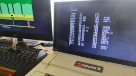
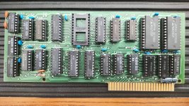
I am in the middle of getting the world's only video about The Frob, a 2600 gamedev system for Apple2, produced.

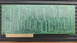
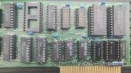
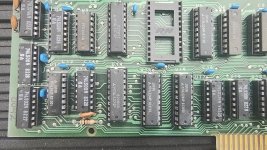
I am at the point where the hardware needs a good reverse engineering, in particular four chips that are privately labeled (PPC350AN), but all have different packages.

As I have CP, I can't do the physical bits needed to do things like removing chips and toning out pins. This is doubly important as this is an exceptionally rare card.

So I'd like to see if someone could help to be my hardware counterpart to reverse engineer this card to document it?

-Thom
 

Attachments

  • rear1.jpg
    rear1.jpg
    592.1 KB · Views: 41
  • front2.jpg
    front2.jpg
    639.5 KB · Views: 41
  • frob_loaded_pitfall.jpg
    frob_loaded_pitfall.jpg
    389.1 KB · Views: 42
  • front1.jpg
    front1.jpg
    651 KB · Views: 38
  • front_full.jpg
    front_full.jpg
    752.3 KB · Views: 33
My gut feeling is that those are PROMs being used as programmable logic devices. IIRC the Frob is old enough that even PALs would be unlikely. Interesting that some of them are in slightly longer packages. Yeah, you'll probably have to make a schematic of everything else to see the context that those chips are in.

At least if they're PROMs, it should be possible to simply run through all the combinations. It's only when there's flip-flop or register logic that it would be difficult. At least being in North Texas you ought to be able to find people nearby who can help.
 
Though not local to you, I'm happy to help out with this because this hardware very much interests me. Unfortunately my comments on your latest video (which, BTW, is not in the Frob playlist) seem to be vanishing, so it's good we can communicate here.

I've started a directory in my retroabandon apple2 repo to collect up information on this. As well as the key pictures above, I've also added the datasheet for the Mitsubishi static RAM ICs.

Unfortunately, the PDFs you linked are difficult to turn back into regular text format; is there any chance you could post here your FMON and AMON listings and, ideally, the source code you're assembling? (Any other source code you have handy will also be welcome.)

Given that I have some idea of how this works already, the photos you provided and getting usable copies of the code will probably let me make some significant progress on the reverse-engineering.
 
Thanks for those!

Also, the photos of the front and back of the Apple 2 peripheral card turn out to be excellent, and I've started in on the reverse-engineering of the Apple 2 peripheral card (you can view progress on the dev/cjs/25c31/frob-mem branch). But it would be good to have an angled pic of the connections underneath the cap on the component side of the board, pins 20-25. (I expect that pin 25, +5V, is connected, and that the rest are not.)

Can you also take similar front/back pictures of the card that plugs into the 2600, and of the end of the cable as it plugs into the Apple II peripheral card? (I am assuming that plugs into J2, the DIP-24W.)
 
@tschak909 I know that user Bolle over at 68k MLA is a wizard when it comes to extracting data from chips, even if they're read-protected with fuses. He's reverse engineered a ton of different accelerator cards, video cards, etc.
 
Well, as you can see in the repo, I've made a bunch of progress on working out hardware details, though in many ways just personal progress on remembering and looking up how the memory maps on the Apple II and the Atari 2600 work and getting pinouts for the various connectors. (The 2600 cartridge pinout was a serious pain; you would not believe how many versions of it on the Internet are wrong in various ways. There are even PCBs out there that simply won't work. I finally took apart one of my carts to confirm that I had it right.)

We now have a list of all the ICs on the Apple II card, along with pinouts and links to datasheets. (Excepting the mysterious DIP-16N "PPC360AN" ones of course.) It's much as one might expect, with some '244s that no doubt switch the SRAMs between the Atari and the Apple, an 8-input NAND gate that's probably doing decoding, and so on. One thing that would be really good to know is if there's any logic on the board that plugs into the Atari cartridge slot, or if it's just a straight connection from the J2 DIP socket.

The board itself is going to need some beeping out, unfortunately. There's too much stuff happening under the ICs and sockets on the front of the board, and even on the back too much stuff going back and forth through vias. But I will be able to figure out a bit of what's going on from the photos.

My next step is to go through the code and see what I can learn from that about how the interactive communication works between the Atari and the Apple. It's not quite as simple as just "switch the SRAM to the Apple II, load it, and switch it to the Atari." It looks, actually, as if the SRAM is being used for communication between the Atari and the Apple II while the Atari is running, which is interesting.
 
Oh man! Sorry, it's always hard circling around when I have dozens of different forums that I am maintaining communication on. :)

---

Cartridge Adapter, it's configured as an 2732 EPROM cartridge PCB. That is to say, an EPROM socket, and a 74LS04 hex inverter for the chip select.

---

I'll attach the Frob manual here. But I'll distill a couple of points:

There are two bi-directional registers exposed, depending on the slot, e.g. for slot 2, these are present at C0A0, and C0A1:

(0) The control and status register

Writes to this register from the apple2 change which 256 byte page is visible in the expansion card window.
Reads act as a status register indicating whether the apple2 or vcs side are ready to receive a byte. Byte 7 is for the VCS side, Byte 6 is for the Apple2 side.

(1) The Data register

This is merely an 8-bit register that either side can read or write to at any time. It acts like a 1 byte dual ported RAM.
The VCS side has to fan out the READ and WRITE for this register to separate addresses due to lack of R/W pin.

These are discussed in Chapter 2 of the Frob Conoisseur's Guide, see attached.

---

There are two programs that use these bi-directional registers, and they use them a bit differently each.

EXPLORER uses the bi-di to read and write ram and registers in the VCS for the Explorer lab. XCONTROL is its Apple2 counterpart.

FMON uses the bi-di to control the VCS for reading, writing memory, as well as setting breakpoints, and preserving processor register states etc for debugging. AMON is its apple2 counterpart.

Frobco provided listings for each of these in the manual, as well.

---

I tried attaching the pdf scan I did of the manual, too large, so google drive link instead. sigh.

What else do you need from me atm? I'm trying to find someone to coordinate with to be "hands" so that the board can be probed.

-Thom
 
Thanks for the manual! I'm glad I got that before I ended up spending much more time reverse-engineering stuff; it explained several things that otherwise I would have had to work out for myself.

I've taken the liberty of uploading the manual to archive.org, mainly because it's larger than I care to put into a repo (almost 40 MB). That also happens to give me an OCR of the text, which I've dumped into the repo and done a bit of cleanup/Markdown formatting on.

Now that I've got all this and have poked around it a bit, I've written an "echo" test program that you should be able to load with FLOAD (2K, upper bank) and test out using the Apple II monitor in the style shown in Chapter 5. After the FLOAD, try writing $F0 to $C0A0 (assuming you're in slot 2) and resetting the VCS, and you should be see that a subsequent read of $C0A0 has bit 6, and reading $C0A1 should give you an ASCII `F` ($46) and $C0A0 should then
have bit 6 clear and bit 7 set. You can then write a value to $C0A1 and you should see the exclusive OR of that value appear when reading that port (i.e., $00 returns $FF, $FF returns $00, etc.).

Looking at your video again, I think the issue there was that you were looking at the wrong routine; 3100 is the write routine in AMON that waits until bit 7 is set in the control register and then writes a value (on line 3110) to the data register.
 

Attachments

Thanks for the manual! I'm glad I got that before I ended up spending much more time reverse-engineering stuff; it explained several things that otherwise I would have had to work out for myself.

I've taken the liberty of uploading the manual to archive.org, mainly because it's larger than I care to put into a repo (almost 40 MB). That also happens to give me an OCR of the text, which I've dumped into the repo and done a bit of cleanup/Markdown formatting on.

Now that I've got all this and have poked around it a bit, I've written an "echo" test program that you should be able to load with FLOAD (2K, upper bank) and test out using the Apple II monitor in the style shown in Chapter 5. After the FLOAD, try writing $F0 to $C0A0 (assuming you're in slot 2) and resetting the VCS, and you should be see that a subsequent read of $C0A0 has bit 6, and reading $C0A1 should give you an ASCII `F` ($46) and $C0A0 should then
have bit 6 clear and bit 7 set. You can then write a value to $C0A1 and you should see the exclusive OR of that value appear when reading that port (i.e., $00 returns $FF, $FF returns $00, etc.).

Looking at your video again, I think the issue there was that you were looking at the wrong routine; 3100 is the write routine in AMON that waits until bit 7 is set in the control register and then writes a value (on line 3110) to the data register.
I added some debugging messages all over FMON, and it seems to fail during the set address, where it sends the command, and then the lo byte of the address, we never get the ok to send the hi byte...

I'll test the echo program in a bit, got source? ;)

-Thom
 
I do find myself wondering, as the data register works as a dual ported register, I am wondering what causes the status bits to go low?

-Thom
 
I do find myself wondering, as the data register works as a dual ported register, I am wondering what causes the status bits to go low?
It might have the appearance of being dual-ported, but it's almost certainly not, despite that they call it "the bi-directional register." The easiest way to implement something like this is as two separate registers, one accessed via read (and write from the other side), and the other accessed via write (and read from the other side). The ready bits can be implemented by setting each one on write to the corresponding port, and clearing each one on read from the corresponding port.

And, if you have a look at the components list, it seems that there's just enough logic for this on the board if we ignore the mysterious PPC360AN chips. We have
  1. U4 and U14, a pair of 74'374 octal (i.e., eight on the IC) latches/flip-flops, which could be used for two directions of the "bi-directional register": actually separate Apple→Atari and Atari→Apple communications registers.
  2. U17, a '174 hex flip-flop, which could be used for the 4-bit page register, the SRAM ownership setting (Apple or Atari) and the bi-directional register enable/disable (probably only on the Atari side), i.e., the lower 6 bits of the control register on the Apple side.
  3. U1, a '174 dual flip-flop, which could be used for the "written but not yet read" bits for the communications registers.
BTW, it just occurred to me, it would also help a bit with working out the design to find out how much decoding they're actually doing on the Apple II registers. I suspect it's just one address bit, but this can be checked in software by seeing if $C0n2 and $C0n3 are mirrors of $C0n0 and $C0n1, and so on, up to $C0nE and $C0nF.
 
Yup, just tested in monitor. Looks like the two registers are mirrored across the whole IO space, all the way up to C0xF.

-Thom
 
  • Like
Reactions: cjs
I started to reverse engineer it from what’s visible in the photos, and it looks like the PPC360AN chips are just a hex buffer of some kind. The pinout matches the normal 74LS36x series so it’s one of those or something very similar.
 
one example from my mess of a schematic - Ax comes from edge connector, RAMAx goes to the SRAM chips:

Screenshot 2025-04-08 at 10.53.22 AM.png
 
  • Like
Reactions: cjs
I might actually be able to finish this schematic with just a few better photos. Basically just need some better top-down views of the left and right sides, so we can see as much of the traces as possible, and the remaining parts that I have to infer, I should be able to verify by knowing how it's supposed to behave.
 
I might actually be able to finish this schematic with just a few better photos. Basically just need some better top-down views of the left and right sides, so we can see as much of the traces as possible, and the remaining parts that I have to infer, I should be able to verify by knowing how it's supposed to behave.
OK, I will get those tomorrow! :)
-Thom
 
I started to reverse engineer it from what’s visible in the photos, and it looks like the PPC360AN chips are just a hex buffer of some kind. The pinout matches the normal 74LS36x series so it’s one of those or something very similar.
one example from my mess of a schematic - Ax comes from edge connector, RAMAx goes to the SRAM chips:
This makes a lot of sense since quite a number of tri-state buffers or similar are needed to switch the SRAM between the Atari and the Apple II. In particular, we need:
  • 8 switches for outgoing Atari data lines (SRAM and Atari read and status ports)
  • 0 switches for incoming Atari data lines (just disable the RAM when the Atari is writing)
  • 12 switches for incoming Atari address lines (SRAM and all Atari ports)
  • 8 switches for incoming Apple data lines (SRAM writes)
  • 8 switches for outgoing Apple data lines (SRAM reads)
  • 8 switches for incoming Apple address lines (SRAM writes, accessed via 256 byte pages)
  • 4 switches for the SRAM bank address lines (unless they're using a '374, which would make sense except that there are are only two '374s and those seem needed for the "bidirectional" data ports. Oh, unless they're putting those in SRAM somehow. But that would be complex...)
It seems odd that they wouldn't use something like a '245 octal bidirectional bus transceiver with tri-state for some of these things, at least the Apple II data lines, though. One of those can replace a pair of '244s, leaving you with only one device for both directions.

Do you have your schematic, or whatever there is of it, on-line somewhere? If you want, I can give you access to the Git repo to put it on a development branch.
 
Back
Top