• Please review our updated Terms and Rules here

TRUE IDE 8-bit XT (XTA) Hard Disk Replacement

Hello, nice to see another enthusiast on Olivetti PCs! I have several (Quaderno, M24, M19, M380XP1, LSX5020, Walkstation/D33) but no Podest PC1 yet (it was not sold in Germany). Your mod also would be interesting for the Quaderno and M19, M24. But until now no chance yet to fix one of my four Quadernos, all have the same problem, no startup. :(
 
I remember the Olivetti's quite well as I worked for a dept that had a pc supply contract with Olivetti. we had Olivetti m21's, 24's, the 286 full height case variations, the 386 full height and wide extra width 386 cases to fit full height mfm/scsi/esdi drives. the m24 pcs we had to upgrade the bios's to support the 40mb drives and upward. my first Olivetti pc started with one 10mb drive which I rapidly filled, so when we upgraded another machine I got a second 10mb drive and had to leave the case open to stack them up - another drive manufacturer around then wasa Conner but I saw those mostly in compaqs - conner made oem versions that Compaq slightly modded firmware to work (better ?) with their systems. also, the Olivetti green screens iirc were a special connector (25pin d ?) so you couldn't attach a non-Olivetti mda, cga etc screen to it unless you changed the video adapter. and while I am doing a brain dump, if anyone has the large 286/386 Olivetti pcs with the heavy duty power supply and large drives, we had to resolder the high current dc connections in the power supply because a medium to heavy load caused dry/cracking joints! I did not come across any quadernos though. aha the M380XP1 - was that one the large, wide case ? the M28, M280 and the M380 were the ones I was referring to with the dry/cracking solder joint problem! it is entirely possible that from the same factory, similar problems may have occurred with the earlier power supplies too.
 
You have 4 all nonfunctional Quaderno's??? The Prodest PC1 was a quite compact machine, that and i'm happy to have an internal mod... it's like a portable PC, now with advantage of an universal TV Connection...
 
Hey, can you explain a couple of things about the wires cut/spliced in the IDE cable? Which signal is pin 27 on the PC1? I was looking at info on the IDE-XT interface and what I've found says it's DACK3 on IBM controllers, but you have it routed to CS1 on the Compact Flash side, so I'm trying to understand what's going on there. Additionally, what is the purpose of bending out the pin on the '2P20' chip? Is there a buffered A2 line coming from the CPU under there? And why does the 2P20 pin need to be tied 'LOW'?

The reason for this is to tie high (+5v) the CS1 line (that is active low) thus disabling it! 2P20 chip is a "gate" for 320-323 I/O addresses that i need to "expand" to 320-327. so i fooled the chip to allow address and also I needed A2 line to be routed to the compact flash!


Also, did you modify the XT-IDE BIOS, or did you use the stock bios? If you modified it, what changes did you make?

I needed to modify the BIOS, of course. First i change the bios address of the hard disk (320h) to another (free) address so the original BIOS is UNAWARE of new hard disk - this was maid because the BIOS pauses and is slow to identify an AT HD. Then i ADDED the "XT-IDE Universal BIOS" in a free place within F000 segment! Then I modified the bios to SEARCH until that area for expansion bios! In that manner there is no problem/conflict with other expansion & VGA BIOSes

I'm just trying to understand this fully because I think it might be a useful mod on the CompuAdd machine I recently got, but since the circuits aren't exactly the same I need to understand why you're making the changes you made so I can apply it to the circuits I do have.

If you have internal ISA slot XT-IDE cards are a very good option. Unless you have to save some slot, of course! Mine (Olivetti PC1) had NO internal slot! :(
 
The reason for this is to tie high (+5v) the CS1 line (that is active low) thus disabling it! 2P20 chip is a "gate" for 320-323 I/O addresses that i need to "expand" to 320-327. so i fooled the chip to allow address and also I needed A2 line to be routed to the compact flash!


I needed to modify the BIOS, of course. First i change the bios address of the hard disk (320h) to another (free) address so the original BIOS is UNAWARE of new hard disk - this was maid because the BIOS pauses and is slow to identify an AT HD. Then i ADDED the "XT-IDE Universal BIOS" in a free place within F000 segment! Then I modified the bios to SEARCH until that area for expansion bios! In that manner there is no problem/conflict with other expansion & VGA BIOSes


If you have internal ISA slot XT-IDE cards are a very good option. Unless you have to save some slot, of course! Mine (Olivetti PC1) had NO internal slot! :(


Looks like I missed your reply, but yes, I went ahead and ordered a Lo-Tech ISA-CF card to install for a 'quick' fix (not really that quick I guess since I have to wait for it to ship from the UK and then self-assemble). I am still interested in attempting to make this work, though, as I'm going to have to put the Lo-Tech card in a bit of an awkward place now that I've actually tried to mount a CF bracket in the machine. The way the CF adapter is mounted on the bracket, it's obviously meant for PCI machines and kind of blocks two of the ISA slots anyway. I am thinking I might just program a GAL similar in configuration to the original PAL in my machine to piggyback on top of it and generate the new address signals (A0 through A9 are all present on the PAL, although A9 is gated with the inverse of the AEN signal before it gets to the PAL for some reason).
 
The reason for this is to tie high (+5v) the CS1 line (that is active low) thus disabling it! 2P20 chip is a "gate" for 320-323 I/O addresses that i need to "expand" to 320-327. so i fooled the chip to allow address and also I needed A2 line to be routed to the compact flash!

Sorry to sort of double-quote, but this line just sank in with me. Are you saying you completely disabled the CS1 line? So the Compact Flash card only responds on CS0 and everything still works just with the expanded address space? If so, that's really interesting and would make the mod simpler compared to what I was thinking would have to be done.

I wish I could just 'fool' the chip I have by removing the A2 line, but I think it might be needed for the other peripherals my chip does address decoding for.
EDIT: Actually, I might be able to. I think the chip I have does address decoding for Serial 1, Serial 2, Parallel, and Game Port (and maybe the Floppy drive, but I'm not sure about that) in addition to IDE, and all of those except IDE do respond on at least eight addresses, so maybe it really would be as simple as re-routing the A2 line.

And regarding the BIOS, I wasn't asking if you modified your computer's BIOS, I was asking if you modified the XT-IDE BIOS in any way. I already knew you had to modify your computer's BIOS, I just didn't know if you had done anything to the XT-IDE bios other than configure it to look at the addresses you needed it to.
 
Last edited:
It will work without CS1, however it does need A2.

That would appear to make things much easier on me.

The PAL in my machine ALREADY outputs 0x320 to 0x327, so that basically means I can just tie CS1 high and splice in A2 and then figure out what to do with IORDY, DRQ, and DACK. This machine also has a separate IDE ROM, so I'd just have to configure the XT-IDE BIOS, burn it to a 27C64, and stick it in the socket where the Western Digital BIOS was.
 
Well, I just tried my idea to see if it would work, and in fact it does not. Or at least it doesn't with the CF card I have. I'll have to see if the CF card works in the Lo-Tech adapter once it gets here.
 
CS1 is used to access the alternate status register and enable device generate intertupts (which aren't used by 8-bit systems).

Re other signals:

  • IORDY - 10k PU
  • IDE D7 - 10k PD (only if buffered at the host)
  • DMARQ - 10k PD
  • CSEL - ground
  • DMACK - leave floating

Note that IDE RESET is active LOW.
 
Last edited:
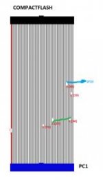
ide mod.jpg
- sorry the image is rendered at very low resolution... this is the link to my guide:
http://www.ti99iuc.it/web/_upload/image/PC1-OnePage/Docs/GuidaCFModPC1HD/sfogliabile_mod_PC1/index.html

That is what I made for my Olivetti Prodest PC1-HD and it worked. The blue line (2P20) is where i get A2 line. My main problem was RESET wich I leaved floating (can be a problem?). Actually this patch is full working, also with dual CF adapter (master/slave).

Are you reading the right value in 320-327h? how is configure XT-IDE universal BIOS?

bye


--- Join my Olivetti Prodest PC1 facebook page: https://www.facebook.com/OlivettiProdestPC1
 
Last edited:
View attachment 24023
- sorry the image is rendered at very low resolution... this is the link to my guide:
http://www.ti99iuc.it/web/_upload/image/PC1-OnePage/Docs/GuidaCFModPC1HD/sfogliabile_mod_PC1/index.html

That is what I made for my Olivetti Prodest PC1-HD and it worked. The blue line (2P20) is where i get A2 line. My main problem was RESET wich I leaved floating (can be a problem?). Actually this patch is full working, also with dual CF adapter (master/slave).

Are you reading the right value in 320-327h? how is configure XT-IDE universal BIOS?

bye


--- Join my Olivetti Prodest PC1 facebook page: https://www.facebook.com/OlivettiProdestPC1

Well, I got 320h through 327h by removing the PAL and testing the address lines on it. The IDE chip select line went LOW from 320h through 327h when the primary/secondary input was set to primary, but interestingly when it was set to secondary, it only responded from 324h to 327h. So I'm not sure why it responds to the full range in one state, but it would appear that it does.

I was actually trying to 'read' the PAL with a microcontroller to see if I could tell exactly what it does, but I was having limited success with that (I only got two of the outputs to actually change state at all and I know this chip is controlling at least five things, and has seven lines that don't appear to be inputs based on where they go on the motherboard).

Maybe I do need to implement the pull-ups and pull-downs like pearce_jj suggested. But I've got a final exam today and a few papers I need to go over again before I print them out, so I probably won't do that today (and in all likelihood, will probably wait until after I can actually test the Lo-Tech card).
 
I finished the microcontroller program to 'read in' the PAL chip in my machine to a CSV file today (over my serial port). Part of the problem I described before was relating to the fact that I was trying to read the PAL with a 3.3V microcontroller. The outputs are 3.3V compliant, but the inputs are not, it seems, so I had to switch to a 5V chip. I know there's already an existing PIC program that does this kind of thing (well, a binary dump that's fed into a special purpose analysis program rather than a CSV), but the author of that program hasn't implemented 24-pin PAL capability yet, so I wrote my own. I imported the CSV into a program called Logic Friday to convert it into equations, then I used those equations to figure out exactly what addresses the chip is responding to. IDE is exactly what my manual testing had already revealed at 320h-327h when Pin 21 is HIGH, and 324h-327h when Pin 21 is LOW. So my addresses are very correct, and it must be something else in my wiring that's causing it not to work properly. Just for fun, since I got this microcontroller project working, I'm going to burn a GAL with the equations I derived and see if it functions just like the original.

EDIT: Ah! I just examined the board and found what at least part of the issue probably is. The CS0 signal goes through a couple of OR gates and a jumper before making it out to the IDE connector. The system manual describes that as the Drive 1/Drive 2 jumper, so I'm thinking that's something to differentiate between the 320-323 range and the 324-327 range when the controller is in Primary mode.
 
Last edited:
I finished the microcontroller program to 'read in' the PAL chip in my machine to a CSV file today (over my serial port). Part of the problem I described before was relating to the fact that I was trying to read the PAL with a 3.3V microcontroller. The outputs are 3.3V compliant, but the inputs are not, it seems, so I had to switch to a 5V chip. I know there's already an existing PIC program that does this kind of thing (well, a binary dump that's fed into a special purpose analysis program rather than a CSV), but the author of that program hasn't implemented 24-pin PAL capability yet, so I wrote my own. I imported the CSV into a program called Logic Friday to convert it into equations, then I used those equations to figure out exactly what addresses the chip is responding to. IDE is exactly what my manual testing had already revealed at 320h-327h when Pin 21 is HIGH, and 324h-327h when Pin 21 is LOW. So my addresses are very correct, and it must be something else in my wiring that's causing it not to work properly. Just for fun, since I got this microcontroller project working, I'm going to burn a GAL with the equations I derived and see if it functions just like the original.
I was thinking to do the same analisys as you... I have a PAL16R8 (the "2P20" chip) and I was thinking to retrieve the equation and modify the chip. What stopped me is that the chip is probably "read-protected" and I needed in every-case (also with modified 2P20 chip) the A2 line... also I don't have the right equipment to read it...


EDIT: Ah! I just examined the board and found what at least part of the issue probably is. The CS0 signal goes through a couple of OR gates and a jumper before making it out to the IDE connector. The system manual describes that as the Drive 1/Drive 2 jumper, so I'm thinking that's something to differentiate between the 320-323 range and the 324-327 range when the controller is in Primary mode.

For sure it switch the Primary/Secondary HD (320-323 range for the first and the 324-327 range for the second). In my case the BIOS try to read 324-327 for the secondary HD but it seem to me that the hardware is not able to support it (the A2 line don't reach the 40 pin connector, or i didn't found it!). Your chip is more complex and can be different from mine. My CS0 line is directly connected to IDEXT...
 
I was thinking to do the same analisys as you... I have a PAL16R8 (the "2P20" chip) and I was thinking to retrieve the equation and modify the chip. What stopped me is that the chip is probably "read-protected" and I needed in every-case (also with modified 2P20 chip) the A2 line... also I don't have the right equipment to read it...

My 'read' method was simply to try every possible input and look at how it affected the output. This way it doesn't matter if the chip is read-protected. It works for mine because it's a PAL20L8, with the 'L' signifying it's not 'registered'. The 'R' in yours means it is registered, so it has a clock signal and flip-flops to deal with, which would make my 'read' method rather ineffective in your case.
 
Well, I gave it one more try today, and unfortunately I still couldn't get it working, even with bypassing those OR gates and adding in the pull-ups/pull-downs, so at this point I don't think there's enough of an advantage in going through the trouble to do this mod 'properly' versus just taking up another ISA slot with the Lo-Tech card. I'll just wait for the Lo-Tech card to come in and just use that instead.
 
Well, I gave it one more try today, and unfortunately I still couldn't get it working, even with bypassing those OR gates and adding in the pull-ups/pull-downs, so at this point I don't think there's enough of an advantage in going through the trouble to do this mod 'properly' versus just taking up another ISA slot with the Lo-Tech card. I'll just wait for the Lo-Tech card to come in and just use that instead.

I'm sorry you had so many problems... in fact I take more than 2 year (I surrender many times then retried) to solve all problems (pearce_jj helped me a lot :) )... what give me faith was the fact that it was my first pc (so internal HD was my childhood dream - and fanless CF card is superb!) and in addition I had no internal ISA slot!

Good luck!
 
Back
Top