Hi,
I got a 16bit ISA controller with 2x COM, 1x LPT, 1x game, 1x IDE, 1x FD.
The datasheet* tells about "Extension Adapter Mode". (Page 44, 46, 59)
This is a stripped down ISA Bus with just 3 address lines.
These are the signals:
/XWR
/XRD
XD0-XD7
XA0-XA2
XIRQ
XDRQ
/XDACK
TC
13 Signals for a basic bus + 3 for DMA.
The datasheet does not tell about speed as far as i can see, there are just timing diagrams which could help estimate, i think.
I simply would have to enable this mode in the controller's configuration registers. After this it's register CR2 is used for holding an user-defined address. Everytime this address matches, A0-A2. D0-D7, RD, WR is going to the DB25 connector.
It looks like it is pretty simple to do IO with 74138 and 8 latches.
I haven't found anything on this EXTADP-mode on the internet, except for a few similar winbond controller datasheets. But these also not telling me more...
My system for testing this controller is a 486-sbc. I disabled the HDC and FDC by jumpers, plugged in, and my system still boots from internal controller, as well as floppy is still working. So now i have to figure out with COM port gets which address (already 2 on the sbc) and IRQ+address jumpers for the LPT.
As the HDC is disabled, there is an GPIO pin free (IDE_D7 / GIO1, pin def datasheet p15) that can be bused as a "general purpose CS"
Datasheet says i can configure an address (GIO1AD0 - GIO1AD10) as well as a decoding mode (GIO1 ADR MODE0/GIO1 ADR MODE1) (page 79, 80, 81).
- 1 byte decode (Compare GIO1ADR10~0 with SA10~0)
- 2 bytes decode (Compare GIO1ADR10~1 with SA10~1)
- 4 bytes decode (Compare GIO1ADR10~2 with SA10~2)
- 8 bytes decode (Compare GIO1ADR10~3 with SA10~3)
I can also configure the type of CS it will be:
" When (AEN=L) & (IOW =L or IOR =L) & (SA10~0=GIO0AD10~0) ,
the pin will be activated. The active level is defined in CR14.bit4
and the IORN or IOWN are defined in CR14.bit3~2. "
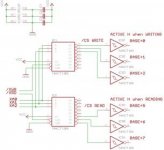
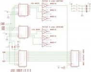
This page http://www.cryogenius.com/hardware/isacard/ shows a simple ISA IO card. My idea is, i could "glue" some prototyping board to that (very small) controller i have and use the address decoder for 2x 74245 + 2x74273 for 16bit IO like shown in last link.
The much simpler thing looks like that EXTADP mode. But i would love to have a bit output port with readback and output-disable (so that i get bi-dir).
Do you guys have any suggestions or maybe a link to information on this EXTADP mode?
I just found a dead link to a program called (W83787 EFDR register reader) http://as.rumia.edu.pl/artur/ftp/bascom/pdf/Interfacing PC/index.html.
* http://pdf.datasheetcatalog.com/datasheets2/17/1793286_1.pdf
* https://4donline.ihs.com/images/Vip...0-1.pdf?hkey=EF798316E3902B6ED9A73243A3159BB0
I got a 16bit ISA controller with 2x COM, 1x LPT, 1x game, 1x IDE, 1x FD.
The datasheet* tells about "Extension Adapter Mode". (Page 44, 46, 59)
This is a stripped down ISA Bus with just 3 address lines.
These are the signals:
/XWR
/XRD
XD0-XD7
XA0-XA2
XIRQ
XDRQ
/XDACK
TC
13 Signals for a basic bus + 3 for DMA.
The datasheet does not tell about speed as far as i can see, there are just timing diagrams which could help estimate, i think.
I simply would have to enable this mode in the controller's configuration registers. After this it's register CR2 is used for holding an user-defined address. Everytime this address matches, A0-A2. D0-D7, RD, WR is going to the DB25 connector.
It looks like it is pretty simple to do IO with 74138 and 8 latches.
I haven't found anything on this EXTADP-mode on the internet, except for a few similar winbond controller datasheets. But these also not telling me more...
My system for testing this controller is a 486-sbc. I disabled the HDC and FDC by jumpers, plugged in, and my system still boots from internal controller, as well as floppy is still working. So now i have to figure out with COM port gets which address (already 2 on the sbc) and IRQ+address jumpers for the LPT.
As the HDC is disabled, there is an GPIO pin free (IDE_D7 / GIO1, pin def datasheet p15) that can be bused as a "general purpose CS"
Datasheet says i can configure an address (GIO1AD0 - GIO1AD10) as well as a decoding mode (GIO1 ADR MODE0/GIO1 ADR MODE1) (page 79, 80, 81).
- 1 byte decode (Compare GIO1ADR10~0 with SA10~0)
- 2 bytes decode (Compare GIO1ADR10~1 with SA10~1)
- 4 bytes decode (Compare GIO1ADR10~2 with SA10~2)
- 8 bytes decode (Compare GIO1ADR10~3 with SA10~3)
I can also configure the type of CS it will be:
" When (AEN=L) & (IOW =L or IOR =L) & (SA10~0=GIO0AD10~0) ,
the pin will be activated. The active level is defined in CR14.bit4
and the IORN or IOWN are defined in CR14.bit3~2. "
This page http://www.cryogenius.com/hardware/isacard/ shows a simple ISA IO card. My idea is, i could "glue" some prototyping board to that (very small) controller i have and use the address decoder for 2x 74245 + 2x74273 for 16bit IO like shown in last link.
The much simpler thing looks like that EXTADP mode. But i would love to have a bit output port with readback and output-disable (so that i get bi-dir).
Do you guys have any suggestions or maybe a link to information on this EXTADP mode?
I just found a dead link to a program called (W83787 EFDR register reader) http://as.rumia.edu.pl/artur/ftp/bascom/pdf/Interfacing PC/index.html.
* http://pdf.datasheetcatalog.com/datasheets2/17/1793286_1.pdf
* https://4donline.ihs.com/images/Vip...0-1.pdf?hkey=EF798316E3902B6ED9A73243A3159BB0