Tronix
Experienced Member
Hello all
and happy new year!
This is my "weekend project" - ISA XT-SD controller. I know about the existence of XT-IDE and IDE-SD adapters. Therefore, there is no problem to use SD card on XT. This project is just a hobby, no more.
So, main idea - use small CPLD for SPI bits shifting:
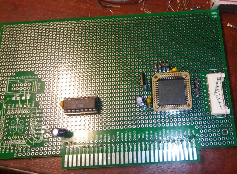
On a board you can see only two IC - 74LS138 as address decoder and EPM3032ALC44-10 CPLD. There is also 1117 linear regulator (5V to 3.3V) and some resistors for SPI pull-up and power filter capasistor 0.1uF. I planned to place here EEPROM memory for additional ROM-BIOS, but too lazy to solder a lot of wires and ordered Lo-tech ISA ROM board.
At the PC side controller have control/status and data ports. Control port used for control SPI CS signal (bit 0), LED (bit 1). Status port are merged with control port. When read control/status port bit 7 indicate INSERT signal from sd-card holder. Bit 6 - SPI BUSY status.
The OUT instruction is used to send data to the SPI
And IN instruction is used for get data from SPI
When previous write cycle not finished and new write attempt occurred, CPLD control CH_IO_RDY signal (make it low) to wait for the previous cycle to complete. When reading data from port CH_IO_RDY signal goes low immediately, MOSI set to 0xFF and shifting begin until bits count = 7. When shifting finished IO_CH_CHK signal goes hi-Z and data present on data bus until /RD signal goes high.
Some diagrams (please dont look at KB_CLK and KB_DATA labels,I forgot to remove them):
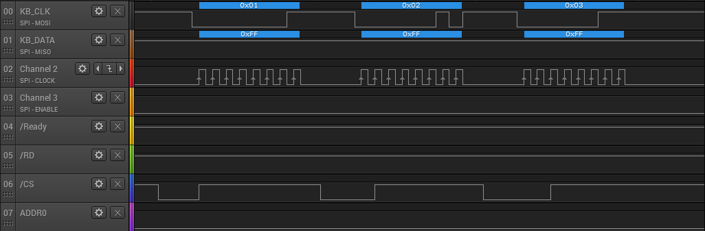
Simple write numbers 1 to 3 with large delays between OUT instructions. CH_IO_RDY (/Ready) signal don't touch
 [/spoiler]
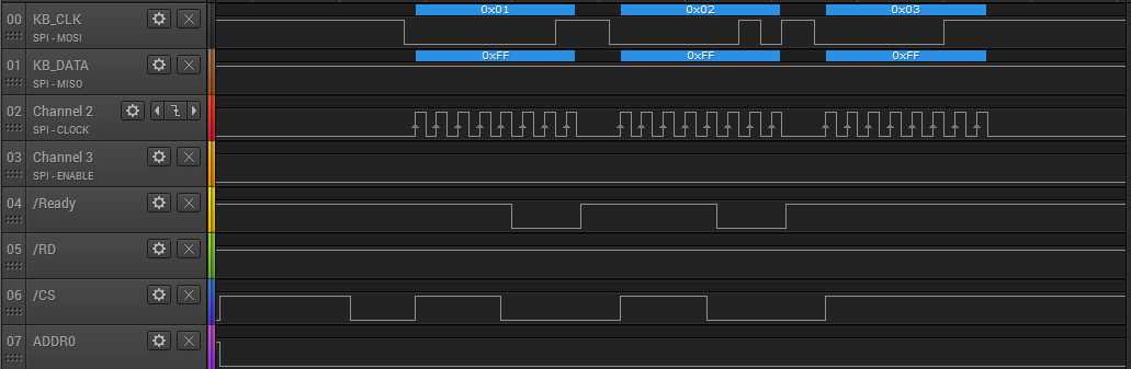
Writing numbers 1 to 3 without delays. CPLD controlled IO_CH_RDY (/Ready) signal:
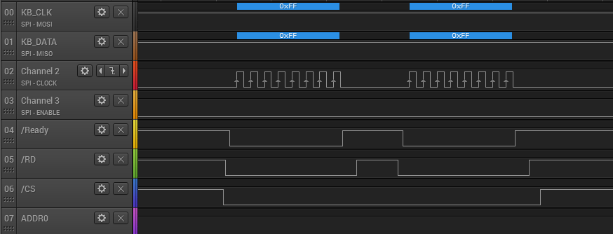
Reading two bytes from SPI:
As a software temp solution i used modified SDPP driver from this forum. So, it's workes:
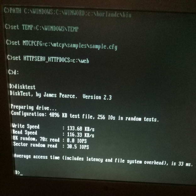
Unfortunately as you will see speed is not too high. At first SDPP driver written in clean C languarge without assembler optimization. This is solved by developing my own additional ROM-BIOS. At second CPLD clocked from CLK ISA signal (8 MHz) and divided by two. So, SPI clock speed is 4 MHz. I tried clocked CPLD from ISA OSC signal (14,3 MHz) without success. I think because they are not synchronized with each other. I just started learning verilog so I do not exclude a bad design. If someone is interested, now here is a verilog code:
and happy new year!
This is my "weekend project" - ISA XT-SD controller. I know about the existence of XT-IDE and IDE-SD adapters. Therefore, there is no problem to use SD card on XT. This project is just a hobby, no more.
So, main idea - use small CPLD for SPI bits shifting:
On a board you can see only two IC - 74LS138 as address decoder and EPM3032ALC44-10 CPLD. There is also 1117 linear regulator (5V to 3.3V) and some resistors for SPI pull-up and power filter capasistor 0.1uF. I planned to place here EEPROM memory for additional ROM-BIOS, but too lazy to solder a lot of wires and ordered Lo-tech ISA ROM board.
At the PC side controller have control/status and data ports. Control port used for control SPI CS signal (bit 0), LED (bit 1). Status port are merged with control port. When read control/status port bit 7 indicate INSERT signal from sd-card holder. Bit 6 - SPI BUSY status.
The OUT instruction is used to send data to the SPI
Code:
out dx,al
Code:
in al,dxWhen previous write cycle not finished and new write attempt occurred, CPLD control CH_IO_RDY signal (make it low) to wait for the previous cycle to complete. When reading data from port CH_IO_RDY signal goes low immediately, MOSI set to 0xFF and shifting begin until bits count = 7. When shifting finished IO_CH_CHK signal goes hi-Z and data present on data bus until /RD signal goes high.
Some diagrams (please dont look at KB_CLK and KB_DATA labels,I forgot to remove them):
Simple write numbers 1 to 3 with large delays between OUT instructions. CH_IO_RDY (/Ready) signal don't touch
Code:
mov al,1
out dx,al
nop
nop
nop
nop
nop
nop
mov al,2
out dx,al
nop
nop
nop
nop
nop
nop
mov al,3
out dx,alWriting numbers 1 to 3 without delays. CPLD controlled IO_CH_RDY (/Ready) signal:
Code:
mov al,1
out dx,al
inc al
out dx,al
inc al
out dx,al
Reading two bytes from SPI:
Code:
in al,dx
in al,dx
As a software temp solution i used modified SDPP driver from this forum. So, it's workes:
Unfortunately as you will see speed is not too high. At first SDPP driver written in clean C languarge without assembler optimization. This is solved by developing my own additional ROM-BIOS. At second CPLD clocked from CLK ISA signal (8 MHz) and divided by two. So, SPI clock speed is 4 MHz. I tried clocked CPLD from ISA OSC signal (14,3 MHz) without success. I think because they are not synchronized with each other. I just started learning verilog so I do not exclude a bad design. If someone is interested, now here is a verilog code:
Code:
module MX2_CPLD(
    // System IO
    input    Clk,              // Input frequency               ISA CLK/ ISA OSC
    input    SysClk,		   // Input frequency				ISA CLK
    input    Res,              // Input reset signal, active 1  ISA RESET
    input    nRD,              // Input read port signal        ISA /IOR
    input    nWR,              // Input write signal            ISA /IOW
    input    nCS,              // Input select controller       from 74138 decoder
    input    Adr,              // Input data/control bus        ISA SA0
    inout    [7:0]Dat,         // Data bus                     	ISA SD0..SD7
    output   Ready,            // Ready                         ISA I/O CH RDY
    // SPI
    output   nSEL,             // Output card select
    output   reg SCK,          // Output SPI frequency
    input    MISO,             // Input SPI data
    output   MOSI,             // Output SPI data
    output   nRED,             // Output LED indicator
    input    nINS              // Input card inserted
);
// Internal registers
reg [7:0]Data;                 // Data register
reg [1:0]Ctrl;                 // Control register
reg [2:0]Bits;                 // Shifted bits counter
reg RMISO;                     // MISO signal latch
reg BUSY;                      // SPI busy
reg MRDY;                  	   // Read/write attempt flag when SPI busy
reg BEGWR;                     // Begin write to data port (falling nWR)
reg BEGWRC;					   // Begin write to control port (falling nWR)
reg BEGRD;                     // Begin read from data port (falling nRD)
// Combinatorics
assign nSEL = ~Ctrl[0];        // Card select
assign nRED = ~Ctrl[1];        // RED LED
assign MOSI = Data[7];         // Output MOSI SPI
assign Dat[7:0] = (~nCS & ~nRD) ?
                    (Adr) ? {~nINS,BUSY,4'h0,Ctrl[1:0]} : Data[7:0]
                    : 8'hZZ;
assign Ready = (MRDY) ? 1'b0 : 1'bZ;  // If read/write attempt when SPI busy down READY signal

// Synchronous logic
always @(posedge Clk) begin
    // Write to control port maybe asynchronous
    if (~nCS & ~nWR & Adr & ~BEGWRC & ~BEGWR & ~BEGRD)
      BEGWRC <= 1'b1;

   if (nWR & BEGWRC)
      begin
         BEGWRC <= 1'b0;
         Ctrl[1:0] <= Dat[1:0];
      end

    // Reset signal high priority
    if (Res)
      begin
         // Clear internal registers
         Ctrl[1:0] <= 2'h0;
         Bits[2:0] <= 3'h0;
         BUSY <= 1'b0;
         SCK <= 1'b0;
         MRDY <= 1'b0;
         BEGWR <= 1'b0;
         BEGWRC <= 1'b0;
         BEGRD <= 1'b0;
         //PRESTART <= 1'b0;
      end
   else
      begin
         // SPI state
         if (BUSY)
            begin
               // SPI working...
               if (SCK)
                  begin
                     // SCK low
                     SCK <= 1'b0;
                     // Falling, shift bits
                     Data[7:0] <= {Data[6:0],RMISO};
                     // Count bits
                     Bits[2:0] <= Bits[2:0] + 3'h1;
                     // This is seven bit?
                     if (Bits[2] & Bits[1] & Bits[0])
                        begin
                           BUSY <= 1'b0;   // Clear BUSY flag
                           MRDY <= 1'b0;   // Goes IO CH RDY to hi-Z
                        end;
                  end
               else
                  begin
                     // SCK high
                     SCK <= 1'b1;
                     // Rising, sample data
                     RMISO <= MISO;
                  end
            end
         else
            begin
               // Clear bits counter
               Bits[2:0] <= 3'h0;
            end

         // Writing to data port (preliminary)
            if (~nCS & ~nWR & ~Adr & ~BEGWR & ~BEGRD & ~BEGWRC)
            begin
               BEGWR <= 1'b1;         // Set preliminary write flag
               if (BUSY)
                  // If SPI busy set IO CH RDY low
                  MRDY <= 1'b1;
            end

         // Final writing to data port (nWR goes high)
         if (nWR & BEGWR)
            begin
            BEGWR <= 1'b0;            // Clear preliminary write flag
            Data[7:0] <= Dat[7:0];       // Grab some data from ISA
            BUSY <= 1'b1;         // Set prestart flag for SPI state machine
            end

         // Reading from data port (preliminary)
            if (~nCS & ~nRD & ~Adr & ~BEGRD & ~BEGWR & ~BEGWRC)
            begin
               BEGRD <= 1'b1;         // Set preliminary read flag
               if (BUSY)
                  // If SPI busy set IO CH RDY low
                  MRDY <= 1'b1;
               else
                  begin
                     MRDY <= 1'b1;             // set IO CH RDY low
                     Data[7:0] <= 8'b11111111;   // 0xFF to data register
                     BUSY <= 1'b1;         // Set prestart flag for SPI state machine
                  end
            end

         // Final reading from data port (nRD goes high)
         if (BEGRD & nRD)
            begin
            BEGRD <= 1'b0;            // Clear preliminary read flag
            // all other job done by combinatorics logic
            end
      end
end

// End
endmodule