• Please review our updated Terms and Rules here

XTIDE with CPLD helper

ian

Member
Joined
Sep 13, 2010
Messages
20
cpld-xtide-cct.jpg

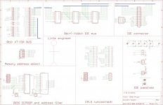
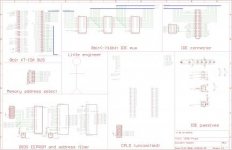
This is the schematic for an XTIDE-compatible XT IDE board. The big difference between this and the XTIDE v1 is that the control logic is built into a single CPLD chip. CPLDs are reprogrammable logic chips that can contain dozens or hundreds of 7400-series style logic. This is a developer friendly board because we can test new designs by uploading a new image, instead of choosing logic chips, routing boards, making PCBs, etc. Later, successful designs can be reimplemented in discrete, through hole logic ICs.

My goal was to fit the entire thing into a big CPLD or FPGA (including bios EEPROM), but there just aren't many 5v parts left. This led to a design for a level-translated universal-bus (XT, Amiga, PCjr, etc), do-all design with a FPGA, but that's for another post. This design uses a small 5V Xilinx FPGA that's still widely available (kind of), and is only $4 in 1sies.
xtide-cpld.jpg

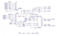
This is the XTIDE drive logic implemented in the CPLD. It uses less than half the available resources, so further improvements are definitely possible.

While the control logic can be changed on the fly, the hard connections cannot. Please let me know if there are other bus pins that would be helpful involve in the logic. DMA? There are a couple free pins on the CPLD, but not many.
 
Last edited:
This looks really interesting, but the ZIP link just gives me numerous different links to adverts.
 
Sorry about that. Any suggestions for a good place to put the file? The forum rejects my .zip (~133K).
 
This looks really interesting, but the ZIP link just gives me numerous different links to adverts.

There is a small line of text at the bottom of the page saying "Save file to your PC: click here". Click on the hyperlink part of it to download the actual file.
 
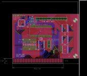
Yup, I'm using a XC9536XL in TQFP, though the huge PLCC package is also common. I'm strange and actually prefer SMD and don't like through-hole at all :) Eagle also limits the board size for the unlicensed version, so SMD helps stay within those constraints as well.

The really BIG 5V CPLDs are also still produced (the kind that could connect to every pin on the bus), but they are really expensive and not usually available in 1sies. I forget the exact count, but integrating everything and the EEPROM into the CPLD would take ~84 pins, and the 100pin FPGAs (max size usually available to consumers) only have 82 pins or something, and they're usually $20+ from 'normal' distributors (Digikey, AVnet).
 
Ian, I think that using something like an Altera MAX7000S CPLD might work better electrically, but nobody would like hand-soldering in a 144-pin TQFP.

I like to hand-prototype my circuits, so I have a pile of various chips mounted to adapter PCBs. But 144 pins was pushing my limit to accommodate that way of operating.
 
TQFP is one of my favorite packages, the more pins the better :) The cost of big CPLDs is really high though, and 5V stuff isn't very future proof. For the 'universal one chip solution' I think FPGA with level translators will be way cheaper. For example, I didn't find the 144 TQFP max7000, but I found this 160pin version with 133 I/Os:
edit///http://search.digikey.com/scripts/DkSearch/dksus.dll?Detail&name=428-1725-ND///
http://search.digikey.com/scripts/DkSearch/dksus.dll?Detail&name=544-2049-ND
It's //48// 60 bucks :( An equivalent 3v3 FPGA with 3->5V translators will probably run <$20, and gives RAM, processing, SPI-reprogrammable (from prompt), etc.

Making the main drive logic reprogrammable for $4, and using another $1 of 7400-series logic for the IDE->XT mux, seemed like a good compromise. It's also a much easier design to deal with, so CPLD novices (like me) can get the logic going before tackling bigger tasks :)
 
Sigh. That seems to be the trend of technology.

Not long ago, I went about pricing a 89C51-series uC and discovered that a 3.3v ARM uC with substantially more memory and I/Os and a faster clock was much cheaper.

You can't fight progress...
 
that's awesome.
so it looks like the eeprom is outside the pld, which is fine. i'm wondering if you had hooked up any other address lines to the ISA connector so that we could use bigger than 8k parts? That's the next thing I'd like to see in the next revision, support for 16 or even 32k parts, so then we could jam all kinds of support into the machine, like HD floppy BIOS routines and eINT13.
 
Are bigger ROM chips the same pinout but using the non-connected pins? I'll have a look now. Any other connections to ISA that would be helpful? There are a few extra pins on the CPLD.
 
I've added a link to your stuff to our wiki.
So, as someone who has a pretty big interest in this stuff, and a number of vintage machines to test it in, what what I need to do to give it a shot? I'm not a hardware guy, so I can't really help with any additional design work, but I can throw some software at it and make sure it's working. I'm also comfy enough with soldering one up if I had the PCB. Mebee shoot me a PM and we can figure something out.
 
CPLDs are fairly easy to program--usually some variation of JTAG or ISP, depending on the vendor. Including a programming header on the board makes for convenience. I like CPLDs a lot. But there are other programmable logic devices that could cut the parts count on the XTIDE and still remain kit-friendly--GALs, for example. Traditional 16- and 20- DIP packages.

It seems that a lot of people will be going to some sort of flash device, so it might also be a consideration to drop the idea of an IDE interface completely and go with something like SDHC. I've been looking into that a bit on my own.
 
My initial reason for using SMD (besides personal preference) is it would be easier to run some off in a pick and place. Just for the pride of manufacturing vintage hardware :)

I like the SDHC idea, and it probably isn't a bottleneck on an old system. It is easier to route... I had a lot of thoughts about using a PIC or FPGA as an intermediary to a cheap serial EEPROM and an SD card when working on the CPLD-enabled XTIDE. Maybe some of that discussion is above.

My basic idea:
Use a big microcontroller (uC) and connect a pin to every bus pin, and connect an SD card and SPI EEPROM. You could even pop on a max232 so you can reprogram the uC with a serial bootloader from the PC serial port (you could also do that with the bus if you can time 9600baud close enough).

The uC could simulate a parallel interface to a cheap (and large) serial EEPROM. I briefly discussed the timing requirements with someone, but don't recall the complete answer. I think 4.77MHZ clock with 4 ticks per operation? Somewhere around 1MHz? The uC will need enough ram to shadow the EEPROM locally if it could even come close to 4.777MHz, but 1MHZ random access might be possible with just a little cache. This might be a good project for an ARM, but it seems overkill and they get expensive with you need a whole bunch of IO.

The SD card part is a breeze compared to emulating an EEPROM. There are plenty of open source SD card librarys that will work, and we get to control the timing. It's just a matter of defining an interface to use between the uC and the bus.

At first I was convinced that using a 5volt part was best, I don't like level translation. Now I think a 3.3volt system will be cheaper and easier. The bus is bidirectional, which is a pain, but the PC controls the direction, and that signal can go directly to a level translator. Many modern 3.3volt parts are 5volt tolerant on some pins, so only the bi-directional pins would need translation. If the XT logic levels are right (>3.0volt=high?) then there would be no need for translation at all (though why not add it to avoid issues...).

These are my disorganized thoughts on that project :) I'd be happy to look closer at chips and designs if you're interesting in the hardware.
 
Do most systems shadow the ROM in RAM, or would the uC have to do double duty emulating the EEPROM and accessing the SD card?
 
Back
Top