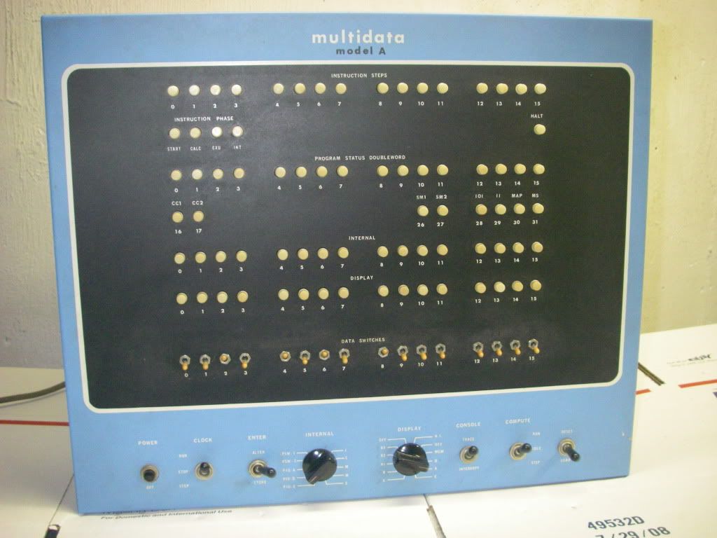
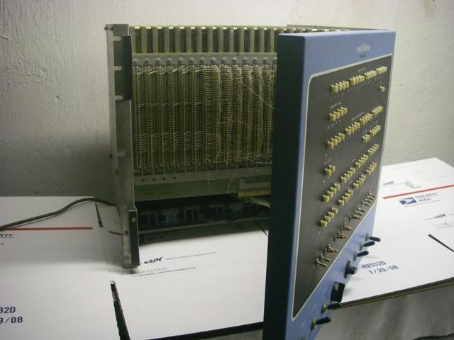
I just aquired this Multidata Model A minicomputer. I made an inquiry on another thread, which lead to a short discussion on Virtual Memory. Here's more information.
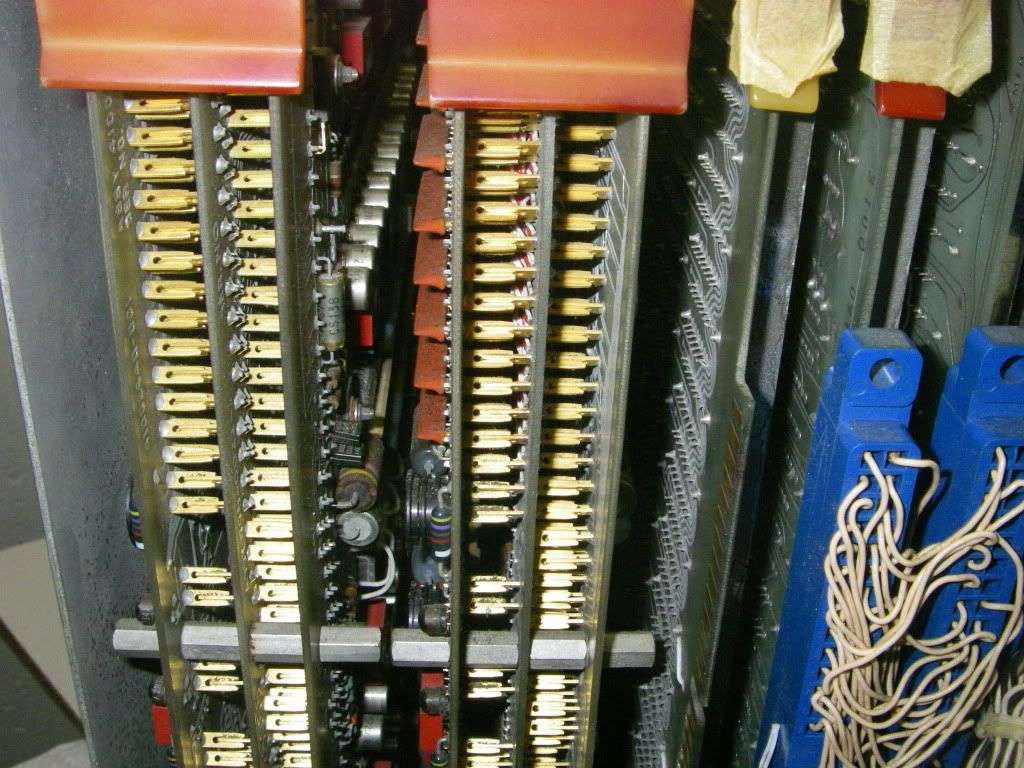
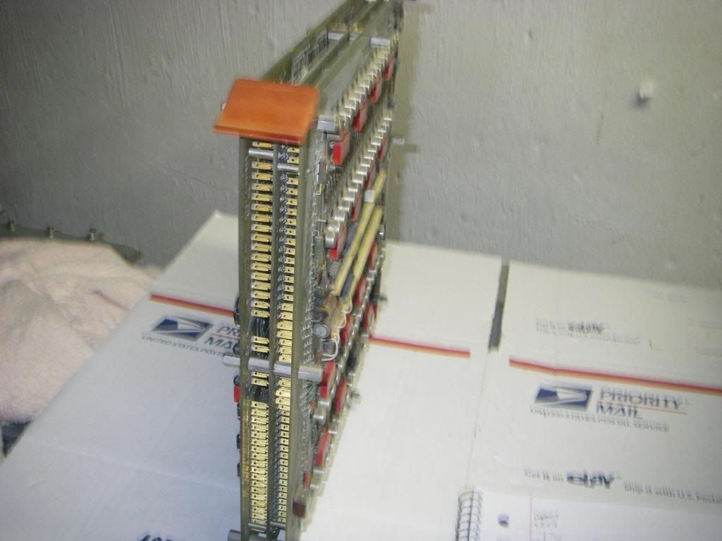
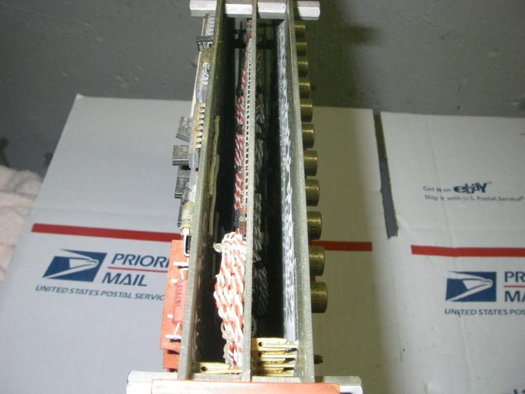
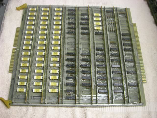
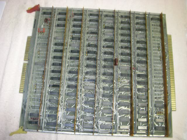
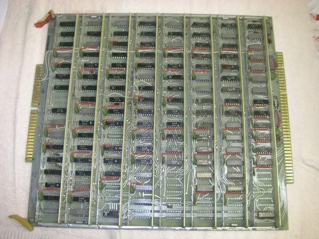
I made this reference board drawing for location purposes
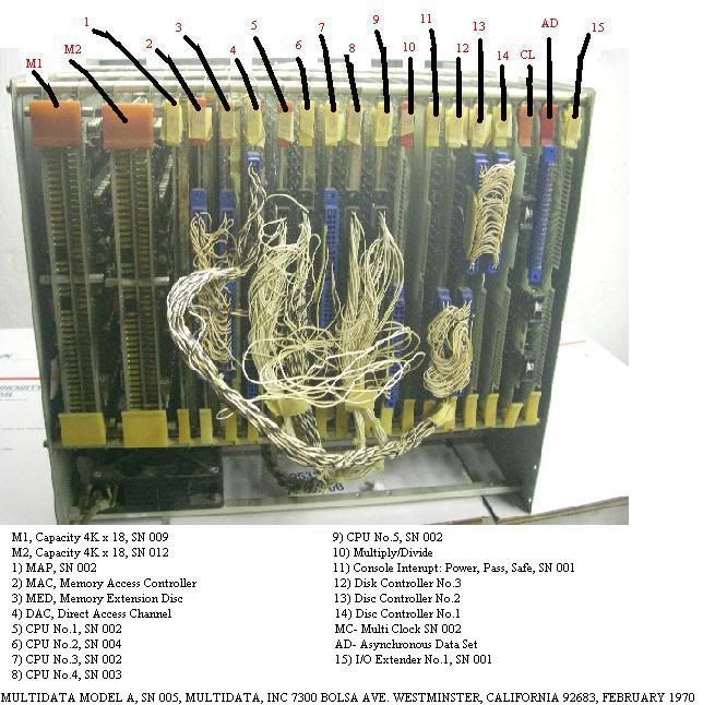
MAP Module
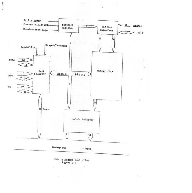
MAC (Memory Access Controller)
MED (Memory Extension Disc)
4k x 18 Core Memory Module (side 1)
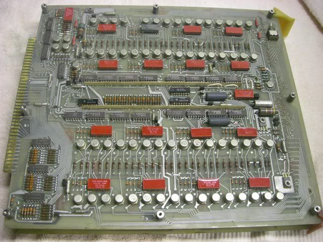
4k x 18 Core memory Module (side 2)
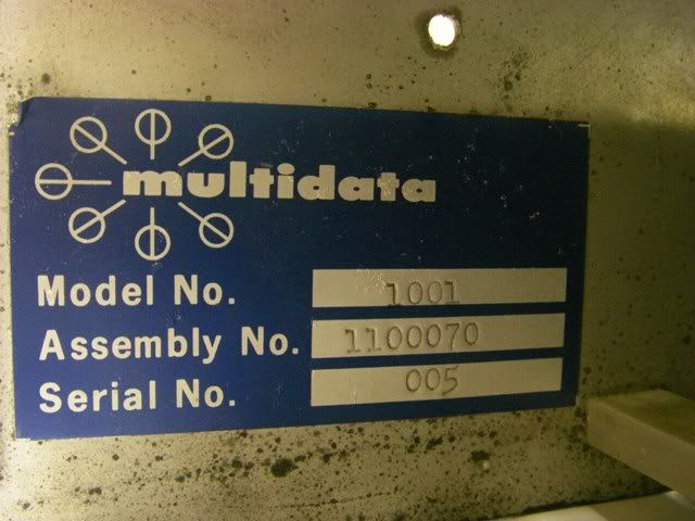
Multidata Model A (Model 1001), Serial No. 005, MA/10 Operating System
February 1970
Memory
Through memory mapping, the Model A executes programs that exceed its core memory capacity.
In the basic configuration the Memory Access Controller (MAC) maps the 32,768-word Memory Extension Disc (MED) into the 4096-word core memory in such a way that the effective capacity of core is equal to that of the disc.
Programmable memory increases to 65,536 words – the range of the 16-bit effective address – in a system with an expanded disc, even if core memory remains at 4096 words.
Memory Access Controller
The Memory Access Controller relieves the programmer of all memory management tasks. It employs a Memory Map to dynamically relocate memory references. And when another program segment needs to be transferred into core, the Kernel initiates the transfer and modifies the Memory Map accordingly. (The Kernel is a small, core-resident program that is always transparent to the user’s program).
The controller provides three dedicated ports to core memory. Data transfers between any port and the memory bus are direct. An address reaches the bus through the Module Selector, which uses the four most significant bits to select the memory module and then loads the twelve least significant bits into the address register of that module.
The Memory Map translates virtual addresses into actual addresses.
The Snapshot Register monitors the eight most significant bits of each address from the processor port for use in error detection.
The interface of the Programmed Input/Output Bus enables the processor to modify the Memory Map to read the Snapshot Register.
Port Selection
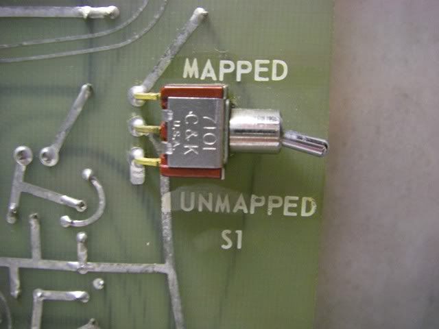
The Memory Extension Disc, the Direct Access Channel, and the Central Processor each have an independent port to core memory. Each port accommodates 16 address lines and 16 data lines. The Port Selector responds to a core memory access request by switching the line from the requesting port into the Memory Access Controller. It resolves simultaneous requests, granting highest priority to the disc port, next highest to the channel port, and lowest to the processor port. Each request indicates whether the access is to be a read or a write and whether the address is to be mapped or unmapped. Thus the disc, the channel, and the processor exercise independent control over the Mapped / Unmapped line, PSW2 controls mapping only while the processor port is selected. (Virtual addresses are always mapped; actual addresses are never mapped).
Mapping
The Memory Access Controller divides core memory into 256-word pages and transfers program segments a page at a time from disc into core. This puts instructions in core, ready for execution.
But the program refers to them by their virtual addresses, which do not agree, in general, with their actual addresses.
The Memory Map solves this problem by keeping track of the correspondence between virtual and actual pages. As a virtual address enters the controller, the Memory Map substitutes the actual page corresponding to the virtual page and thereby produces the actual address.
The Memory Map is a compliment of 128 (optionally 256) 10-bit integrated circuit registers, one for each page of virtual memory.
The Memory Map needs updating every time a virtual page changes status. To modify the contents of a map register, the Kernel sets up to the desired configuration in the ten least significant bits of the D register.
Core Memory
As many as 16 Core Memory modules operate independently on an asynchronous memory bus. The full memory cycle takes 880 nanoseconds. Each module contains 4096 words and has its own address and data registers. These registers allow the bus to release early and thereby overlap successive memory access to different modules.
Memory Extension Disc
Programs written for virtual memory are stored on the Memory Extension Disc. These programs may occupy any combination of 256-word pages, but they normally take contiguous pages in program sequence. Disc capacity may be 32,768 words, 65,536 words or 131,072 words. A single program may not exceed 65,536 words, the range of the 16-bit effective address, but a disc may hold programs to the limit of its capacity.
In its basic configuration the disc has 16 tracks, with 8 sectors per track and 256 words per sector. Expansion simply increases the number of tracks (to either 32 or 64) on the same side of the disc.
A fixed-head, head-per-track design holds the average access time to 16.67 milliseconds (one-half of the rotational period of the disc). The heads ride on a cushion of air and do not contact the recording surface. This flying head feature increases reliability, particularly during startup and shutdown.
The disc controller generates odd parity while writing a sector on disc and checks it while reading.
Central Processor
The Central Processor provides the programmer with the means to make full use of comprehensive instruction repertoire: addressable registers, condition codes, operating modes, double indexing, indirect indexing, and relative indexing forward and backwards.
Rapid context switching assures efficient handling of interrupts and smooth changes in operating mode.
The memory reference instructions operate directly on eight full-word registers. These addressable registers occupy either the first eight core memory locations or (optionally) 128 integrated circuit flip-flops. Either way, they are always addressable as absolute locations 0-7. (Effective addresses in this range are not mapped).
Program Status Doubleword
By keeping a summary of the program environment in two 16-bit integrated circuit registers, the Program Status Doubleword enables the Model A to transfer control quickly from one program to another. This ability to turn suddenly to a new program and provide it with its correct operating environment, called rapid context switching, makes the Multidata Model A especially efficient in handling interrupts and in transferring control back and forth between user programs and the operating system.
Rapid context switching is implicit in traps, interrupts, and the execution of a Call 1 or a Call 2 instruction. The occurance of any of these events will automatically cause the current Program Status Doubleword to be swapped for the one pertaining to the subroutine being called. Later, in exiting from this subroutine, the Branch Return and Clear instruction will put the previous Program Status Doubleword back in control.
-------------------------------------------------------------------------------------------------
Multidata, Inc. Model A, (Model 1001) Serial No. 005, February 1970
The salient characteristics of the Multidata Model A, MA/10 Operating System are:
• 32,768 words of programmable memory, expandable to 65,536 words
• Memory map
• Automatic program fragmentation
• Dynamic program relocation
• Memory write protection
• 880-nanosecond core memory cycle time
• 4096-word core memory, expandable to 65,536 words
• 32,768-word memory extension disc, expandable to 131,072 words
• Rapid context switching
• Eight addressable registers
• Double indexing
• Single-level indirect addressing
• Privileged instruction
• Five-bit operation field
• Only single-word instructions
• User-defined instructions
• Relative addressing, forward and backward
• IOP-oriented input/output system
• Multilevel interrupt system
• Device independent input/output
• Up to 384 individually armed, enabled, triggered, sensed and set interrupts
• Multiple real-time clocks
• Remote control panel
• Asynchronous, demand-multiplexed input/output
• Data chaining
• Command chaining
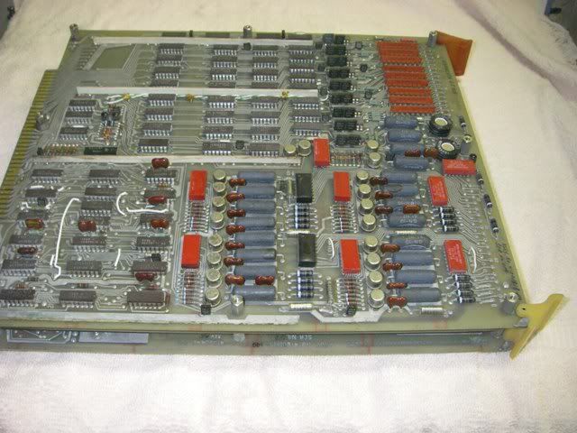
I made this reference board drawing for location purposes
MAP Module
MAC (Memory Access Controller)
MED (Memory Extension Disc)
4k x 18 Core Memory Module (side 1)
4k x 18 Core memory Module (side 2)
Multidata Model A (Model 1001), Serial No. 005, MA/10 Operating System
February 1970
Memory
Through memory mapping, the Model A executes programs that exceed its core memory capacity.
In the basic configuration the Memory Access Controller (MAC) maps the 32,768-word Memory Extension Disc (MED) into the 4096-word core memory in such a way that the effective capacity of core is equal to that of the disc.
Programmable memory increases to 65,536 words – the range of the 16-bit effective address – in a system with an expanded disc, even if core memory remains at 4096 words.
Memory Access Controller
The Memory Access Controller relieves the programmer of all memory management tasks. It employs a Memory Map to dynamically relocate memory references. And when another program segment needs to be transferred into core, the Kernel initiates the transfer and modifies the Memory Map accordingly. (The Kernel is a small, core-resident program that is always transparent to the user’s program).
The controller provides three dedicated ports to core memory. Data transfers between any port and the memory bus are direct. An address reaches the bus through the Module Selector, which uses the four most significant bits to select the memory module and then loads the twelve least significant bits into the address register of that module.
The Memory Map translates virtual addresses into actual addresses.
The Snapshot Register monitors the eight most significant bits of each address from the processor port for use in error detection.
The interface of the Programmed Input/Output Bus enables the processor to modify the Memory Map to read the Snapshot Register.
Port Selection
The Memory Extension Disc, the Direct Access Channel, and the Central Processor each have an independent port to core memory. Each port accommodates 16 address lines and 16 data lines. The Port Selector responds to a core memory access request by switching the line from the requesting port into the Memory Access Controller. It resolves simultaneous requests, granting highest priority to the disc port, next highest to the channel port, and lowest to the processor port. Each request indicates whether the access is to be a read or a write and whether the address is to be mapped or unmapped. Thus the disc, the channel, and the processor exercise independent control over the Mapped / Unmapped line, PSW2 controls mapping only while the processor port is selected. (Virtual addresses are always mapped; actual addresses are never mapped).
Mapping
The Memory Access Controller divides core memory into 256-word pages and transfers program segments a page at a time from disc into core. This puts instructions in core, ready for execution.
But the program refers to them by their virtual addresses, which do not agree, in general, with their actual addresses.
The Memory Map solves this problem by keeping track of the correspondence between virtual and actual pages. As a virtual address enters the controller, the Memory Map substitutes the actual page corresponding to the virtual page and thereby produces the actual address.
The Memory Map is a compliment of 128 (optionally 256) 10-bit integrated circuit registers, one for each page of virtual memory.
The Memory Map needs updating every time a virtual page changes status. To modify the contents of a map register, the Kernel sets up to the desired configuration in the ten least significant bits of the D register.
Core Memory
As many as 16 Core Memory modules operate independently on an asynchronous memory bus. The full memory cycle takes 880 nanoseconds. Each module contains 4096 words and has its own address and data registers. These registers allow the bus to release early and thereby overlap successive memory access to different modules.
Memory Extension Disc
Programs written for virtual memory are stored on the Memory Extension Disc. These programs may occupy any combination of 256-word pages, but they normally take contiguous pages in program sequence. Disc capacity may be 32,768 words, 65,536 words or 131,072 words. A single program may not exceed 65,536 words, the range of the 16-bit effective address, but a disc may hold programs to the limit of its capacity.
In its basic configuration the disc has 16 tracks, with 8 sectors per track and 256 words per sector. Expansion simply increases the number of tracks (to either 32 or 64) on the same side of the disc.
A fixed-head, head-per-track design holds the average access time to 16.67 milliseconds (one-half of the rotational period of the disc). The heads ride on a cushion of air and do not contact the recording surface. This flying head feature increases reliability, particularly during startup and shutdown.
The disc controller generates odd parity while writing a sector on disc and checks it while reading.
Central Processor
The Central Processor provides the programmer with the means to make full use of comprehensive instruction repertoire: addressable registers, condition codes, operating modes, double indexing, indirect indexing, and relative indexing forward and backwards.
Rapid context switching assures efficient handling of interrupts and smooth changes in operating mode.
The memory reference instructions operate directly on eight full-word registers. These addressable registers occupy either the first eight core memory locations or (optionally) 128 integrated circuit flip-flops. Either way, they are always addressable as absolute locations 0-7. (Effective addresses in this range are not mapped).
Program Status Doubleword
By keeping a summary of the program environment in two 16-bit integrated circuit registers, the Program Status Doubleword enables the Model A to transfer control quickly from one program to another. This ability to turn suddenly to a new program and provide it with its correct operating environment, called rapid context switching, makes the Multidata Model A especially efficient in handling interrupts and in transferring control back and forth between user programs and the operating system.
Rapid context switching is implicit in traps, interrupts, and the execution of a Call 1 or a Call 2 instruction. The occurance of any of these events will automatically cause the current Program Status Doubleword to be swapped for the one pertaining to the subroutine being called. Later, in exiting from this subroutine, the Branch Return and Clear instruction will put the previous Program Status Doubleword back in control.
-------------------------------------------------------------------------------------------------
Multidata, Inc. Model A, (Model 1001) Serial No. 005, February 1970
The salient characteristics of the Multidata Model A, MA/10 Operating System are:
• 32,768 words of programmable memory, expandable to 65,536 words
• Memory map
• Automatic program fragmentation
• Dynamic program relocation
• Memory write protection
• 880-nanosecond core memory cycle time
• 4096-word core memory, expandable to 65,536 words
• 32,768-word memory extension disc, expandable to 131,072 words
• Rapid context switching
• Eight addressable registers
• Double indexing
• Single-level indirect addressing
• Privileged instruction
• Five-bit operation field
• Only single-word instructions
• User-defined instructions
• Relative addressing, forward and backward
• IOP-oriented input/output system
• Multilevel interrupt system
• Device independent input/output
• Up to 384 individually armed, enabled, triggered, sensed and set interrupts
• Multiple real-time clocks
• Remote control panel
• Asynchronous, demand-multiplexed input/output
• Data chaining
• Command chaining