Upcoming Events:
- VCF South West - June 14 - 16, Davidson-Gundy Alumni Center at University of Texas at Dallas
- VCF West - Aug 2 - 3, Computer History Museum, Mountain View, CA
- VCF Midwest - Sept 7 - 8 2024, Schaumburg, IL
- VCF SoCal - Mid February 2025, Location TBD, Southern CA
- VCF East - April 2025, Infoage Museum, Wall NJ
-
Please review our updated Terms and Rules here
You are using an out of date browser. It may not display this or other websites correctly.
You should upgrade or use an alternative browser.
You should upgrade or use an alternative browser.
PET 2001-8 Video Display Dead
- Thread starter wbochar
- Start date
dave_m
Veteran Member
I was reading the pins off of J8 right out of the connector, using the middle black pin and measuring out to each of the pins. But as I read it today, the inner pins measured against ground (middle) is 4.6VAC.
I am confused. By "inner pins" do you mean the red wires from the big capacitor? If J8 is connected to the board, they pick up the 1/2 wave rectifier diodes and should measure at least 8VDC. Remember to use the DC scale for the red wires.
MikeS
Veteran Member
Yes, it's wired correctly but your readings don't sound right; as Dave points out, we're looking for around 8VDC between pin3 and pins 2 and 4 of the connector, and around 8VAC between pin 3 and pins 1 and 5. (VA means Volt-Amps, which is Volts times Amps, often equivalent to Watts and not relevant here). If you really are only reading around 7.5V that might indicate something drawing excessive power somewhere, especially with that one VR outputting <5V. If you really are reading 4.6VAC on the red wires that might indicate a bad diode and also explain the low voltage; what does the scope show on pins 2 and 4 of J8?Is this wired correctly?
I would have left the green and white wires for the time being; the power connector is really inadequate for the current going through it and is a common failure point.
Nevertheless, we are getting close to 5V on the four Vcc lines...
The jumper between J9-6 and H9-1 is interesting; it's presumably replacing a trace that is missing, broken or corroded. Can you see what the reason for it is, and are there any other jumpers or signs of corrosion?
Last edited:
I am confused. By "inner pins" do you mean the red wires from the big capacitor? If J8 is connected to the board, they pick up the 1/2 wave rectifier diodes and should measure at least 8VDC. Remember to use the DC scale for the red wires.
This is really weird, I keep getting different signals.When I powered up without anything connected, I was getting half the voltage at 4.2VDC. I popped the J8 male connector and adjusted pin holders, checked/tugged the cables then powered the system and now its outputting 8.96VDC. I guess the connections out of the big capacitor were not stable (or the capacitor is wonky).
Measuring the voltages across the board again, without the added power lines. Any chip around J8 has 5VDC, as it expands out in a semi circle the voltage drops to 4.91VDC at the corners (Tape Connector/Expansion and last bank of Ram). I've noticed the ROM Bank closer to J8 is warmer than the rest.
The voltage regulators:
Row A : 4.93 VDC
Row C: 5.0 VDC
Row D: 4.93 VDC
Row F: 4.93 VDC
But reading Chip voltages in Rail C, everything hovers around 4.91 VDC.
MikeS
Veteran Member
If J8 is disconnected you won't get any DC voltage at all, so you might just have been measuring residual voltage on the capacitor.This is really weird, I keep getting different signals.When I powered up without anything connected, I was getting half the voltage at 4.2VDC.
The voltages sound close enough, so we may well be off on an irrelevant tangent...
The jumper between J9-6 and H9-1 is interesting; it's presumably replacing a trace that is missing, broken or corroded. Can you see what the reason for it is, and are there any other jumpers or signs of corrosion?
I assumed that jumper was part of the original board. This is first time for me seeing the inside of this model.
I noticed a broken/corroded trace going to H8 PIN 1, so I jumpered that a while back. Should I get rid of the other jumper?
MikeS
Veteran Member
As long as you have a good connection between J9-6, pin 1 of both H8 and H9, and pin 10 of all the 2114 RAM chips it should be OK.I noticed a broken/corroded trace going to H8 PIN 1, so I jumpered that a while back. Should I get rid of the other jumper?
But I'd inspect the board carefully for any other broken/corroded traces. This could indeed be a challenging board... ;-)
Also, can you confirm whether or not you really have an AC voltage on the +8VDC line(s) (the red wires on J8-2 and J8-4) ?
And are the screws on the capacitor nice and tight?
Last edited:
As long as you have a good connection between J9-6, pin 1 of both H8 and H9, and pin 10 of all the 2114 RAM chips it should be OK.
But I'd inspect the board carefully for any other broken/corroded traces. This could indeed be a challenging board... ;-)
Also, can you confirm whether or not you really have an AC voltage on the +8VDC line(s) (the red wires on J8-2 and J8-4) ?
And are the screws on the capacitor nice and tight?
Set my DVM for VAC,
j8-2 + j8-4 0VAC.
J8-2 + J8-3 7.1VAC
j8-4 + J8-3 7.1VAC
MikeS
Veteran Member
Again,Set my DVM for VAC,
j8-2 + j8-4 0VAC.
J8-2 + J8-3 7.1VAC
j8-4 + J8-3 7.1VAC
andwhat does the scope show on pins 2 and 4 of J8?
are the screws on the capacitor nice and tight?
I replaced the J8 Connector and Socket to the board. Things look better.
My DSO Scope is working after a small fix to the tuning section and a re calibration.
There is no AC on the DC lines J8 PIN2&4.
Voltage Regulator Outputs:
Row A : 4.93 VDC
Row C: 5.0 VDC
Row D: 4.93 VDC
Row F: 4.93 VDC
5V off the internal tape connector
and 4.91V off the external tape connector
The Power output from 5-4.91V depending on how far out you are from the J8 Connector.
E2-PIN6 is Flatlined, no pattern with the scope.
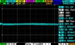
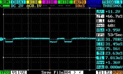
Horizontal Drive is getting this in short bursts:
I checked all the traces and couldn't find anything broken.
My DSO Scope is working after a small fix to the tuning section and a re calibration.
There is no AC on the DC lines J8 PIN2&4.
Voltage Regulator Outputs:
Row A : 4.93 VDC
Row C: 5.0 VDC
Row D: 4.93 VDC
Row F: 4.93 VDC
5V off the internal tape connector
and 4.91V off the external tape connector
The Power output from 5-4.91V depending on how far out you are from the J8 Connector.
E2-PIN6 is Flatlined, no pattern with the scope.
Horizontal Drive is getting this in short bursts:

I checked all the traces and couldn't find anything broken.
dave_m
Veteran Member
E2-PIN6 is Flatlined, no pattern with the scope.
No buffered 8 MHz at pin 6? Try the input at E2-pin 5. If this is not a 8 MHZ square wave then the oscillator circuit may be bad. Your DSO does not sample well enough to see 8 MHZ cleanly but you should see a high frequency signal.
No buffered 8 MHz at pin 6? Try the input at E2-pin 5. If this is not a 8 MHZ square wave then the oscillator circuit may be bad. Your DSO does not sample well enough to see 8 MHZ cleanly but you should see a high frequency signal.
It's flat with the occasional very slight dip into the negative. If I switch to DC0.5V increments it looks like a -.2V to 0.
dave_m
Veteran Member
It's flat with the occasional very slight dip into the negative. If I switch to DC0.5V increments it looks like a -.2V to 0.
Let's look at the inverter amplifiers in the oscillator circuit: D9-pins 8,9,10 and 11.
Let's look at the inverter amplifiers in the oscillator circuit: D9-pins 8,9,10 and 11.
D9- 8,9,10 Slight positive value but flat
D9- 11 Tight square wave around 1v
dave_m
Veteran Member
D9- 8,9,10 Slight positive value but flat
D9- 11 Tight square wave around 1v
To me, it seems the crystal is trying to do its thing, but the inverters are bad. Piggyback a 74LS04 on D9 to see if things get better. If so, replace the D9 inverter chip (74LS04). There is supposed to to a test point called TP2-1 that monitors the 8 MHZ. See if you can find it, or just look at D9-pin8.
MikeS
Veteran Member
Makin' progress; excellent!
dave_m
Veteran Member
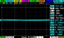
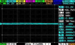
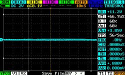
Replaced,
Getting signals on all pins.
That just looks like a little noise on a static zero to me. What is the vertical scale in volts per division and are you using a 10X probe or not? What is the zero volt line? Remember anything less than 0.4V is a logic zero. Anything above 2.4V is a logic one regardless of a little noise on it.
-Dave
2V/Div x1 probes, zero line is the middle of the grid vertically.

