• Please review our updated Terms and Rules here

Building the Multicomp CP/M FPGA Computer

JonB

Veteran Member
Joined
Jan 26, 2014
Messages
1,652
Location
South Herefordshire, UK
Hi All

Before we begin, I want to call out a big thanks to Grant Searle, who has shown us how to build a computer easily and cheaply using FPGA. Thank you Grant for another excellent and educational guide! All works referred to here are Grant's copyrighted stuff and the credit belongs to him.

In this thread I am going to discuss building Grant Searle's Multicomp CP/M FPGA computer. I received a PM from a member enquiring after it, and needed somewhere to post pictures.

The story begins with a visit to Grant Searle's Multicomp web page: http://searle.hostei.com/grant/Multicomp/

As you can see, it offers several options for configuring an Altera Cyclone II FPGA board for running an emulated 8 bit computer. For a CP/M capable configuration, you will need the Z80 option with Full RAM.

You now need to acquire some parts:

  • Altera Cyclone II EP2C5T144 like this one: http://www.ebay.co.uk/itm/272110247623
  • Altera USB blaster (device for programming the Cyclone II board - note it's included in the above listing).
  • Stripboard, pin headers and jumper cables for making the carrier board for the additional RAM (plus optional VGA/PS2 interface) carrier boards.
  • AS6C1008 SRAM chip plus DIL socket (required for CP/M) - it's the "Full RAM option" described on the web page.
  • A USB - RS-232 breakout board or adapter. Note, it must support hardware handshaking CTS/RTS.
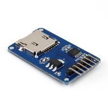
  • SD card socket with header pins (I used a micro SD card adapter and soldered pins directly to it).
  • Downloaded Altera Quartus II software for programming the Cyclone II board. Careful here, later versions aren't compatible with the Cyclone II, you need this one: https://dl.altera.com/13.0sp1/?edition=web
  • A 5v power supply with a plug that is compatible with the Cyclone II board's power socket (or you can drive it from the USB RS232 adapter if it provides 5v).

None of this is terribly expensive. You also need some moderate soldering skills (for making the carrier boards) and dexterity (for connecting it all together).

IMG_0939.jpgJumpers and Headers.jpgIMG_1435.jpg
 
Last edited:
Making the SRAM carrier board.

Cut a piece of stripboard big enough for the 32 pin DIL socket, allowing an additional 7 strips on one side (we'll use these for some power distribution) and say 5 holes either side of the DIL socket. Solder the socket to the strip board with the strips running across the socket. Then cut the strips in the middle of the socket so that the let and right row of pins are not connected to each other. Then add a strip of header pins to each side. You are looking to be able to connect jumper leads to each of the pins of the socket.

Here are some pictures. The first one shows the carrier board with the SRAM fitted, wired to the FPGA board. The second one shows the underside of the carrier board and is far more instructive. You can see where the strips are cut in between the legs of the SRAM's socket and the outer rows of solder blobs are for the header pins. To the left (where my thumb is) are a couple of additional rows of header pins that I am using to implement the +5v-Vcc-CS2 connection shown on Grant's page (I also used it as a power distribution point previously).

IMG_1430.jpgIMG_1431.jpg
 
Last edited:
The optional PS2/VGA Carrier board.

A little thought is needed when building this carrier board. You don't need it if you are going to use your PC and a serial adapter to talk to the machine. I designed the layout from Grant's schematic and wired a flying PS2 adapter (taken from a lead I had lying about) and VGA socket. Again, using header pins to facilitate connectivity with the FPGA board.

A close up..

IMG_1429.jpg
 
Last edited:
The SD card adapter.

In order to connect an SD card, I chose to utilise a micro SD card adapter that I had lying around, and solder header pins directly to its contacts. Thus my machine has a microSD card plugged into the adapter.

IMG_1432.jpgIMG_1433.jpg
 
Wiring it up and programming the board

As you can see from the pictures, the wiring is fairly easy. All you need to do is use the jumpers to connect pin to pin (FPGA board to carrier board) as shown in Grant's diagram. To build a CP/M capable machine, you require the Full RAM option and one serial port adapter. Follow the instructions on Grant's page, methodically working your way round the board. Double check everything.

To program the board, you need the Quartus II software installed on your PC. Load the VHDL from Grant's page and modify it as he describes for a Z80 machine. Take your time and work from the top to the bottom of the VHDL section. Choose the lower clock speed initially (you can change this later once the machine is working). It is a matter of starting with the "breadboard", which is a VHDL skeleton file and pasting the options you want into the relevant sections of the breadboard file. Chose all sections ("blocks") labelled for the Z80, plus the additional RAM, SD card and serial port.

Grant assumes you will be able to work out how to compile the VHDL and load it to the board. It's not too hard to work out using the Quartus II software and USB Blaster device so I'm going to leave that to you for now (plus, I'm away from the PC I used at the moment).
 
JonB,
I have been looking over the information again, and I've got a couple of questions.

1. Is it possible to use one of these SDCard adapters versus soldering direct to a SDCARD?

http://www.mouser.com/ds/2/272/mmc_proto_manual_v100-469614.pdf
http://www.mouser.com/ds/2/321/32313-SDCardAdapter-v1.1-472828.pdf
http://www.mouser.com/Search/ProductDetail.aspx?qs=Vxac6xGyzPmXcjDQfYwAEg==
https://www.adafruit.com/products/254?gclid=COGr1_KCss4CFQGOaQodtzAFbQ

2. What is the Pinout of the SDCard for the wiring Grant used?

I've downloaded lots of Photo's and there are several different pinouts that are shown?

3. What are the names of the Software Code Signals on P2 that correspond to the wires going to the SDCard,
and where are these defined in the actual code. I've not found it yet. I thought it would be in the
USART code. Just references to the standard library.

4. What is a good source for the Memory IC?

Thanks.


Larry
 
FWIW, I use the commodity MicroSD adapters available on eBay and Aliexpress. They're cheap (about $1 each), have clearly labeled pins and include a 5V-to3.3v LDO regulator (can be bypassed if you already have 3.3V). They're micro SD, not full-size SD, but in today's world, it's usually easier to buy the micros and then use an adapter if the larger size is needed. Just don't lose the things in your morning cornflakes.

New-Arrival-Mciro-SD-TF-Card-Memory-Shield-Module-SPI-Micro-SD-Storage-Expansion-Board-For.jpg_220x220.jpg
 
This is a really cool project. I had not seen the MultiComp previously, but definitely want to build one now. Very neat!
 
This is a really cool project. I had not seen the MultiComp previously, but definitely want to build one now. Very neat!

There are a few FPGA versions of CP/M projects out there, some complete others not.

I think one by Howard Harte, and he has an EZ80 version of a CP/M machine.

That was some time back.

I should bring up both since I have a couple of EZ80 development kits and a couple FPGA development boards doing nothing.


Randy
 
JonB,
I have been looking over the information again, and I've got a couple of questions.

1. Is it possible to use one of these SDCard adapters versus soldering direct to a SDCARD?

http://www.mouser.com/ds/2/272/mmc_proto_manual_v100-469614.pdf
http://www.mouser.com/ds/2/321/32313-SDCardAdapter-v1.1-472828.pdf
http://www.mouser.com/Search/ProductDetail.aspx?qs=Vxac6xGyzPmXcjDQfYwAEg==
https://www.adafruit.com/products/254?gclid=COGr1_KCss4CFQGOaQodtzAFbQ

2. What is the Pinout of the SDCard for the wiring Grant used?

I've downloaded lots of Photo's and there are several different pinouts that are shown?

3. What are the names of the Software Code Signals on P2 that correspond to the wires going to the SDCard,
and where are these defined in the actual code. I've not found it yet. I thought it would be in the
USART code. Just references to the standard library.

4. What is a good source for the Memory IC?

Thanks.


Larry

Hello Larry, here are some replies for you.

1. I think so - see Chuck's reply. The board is running at 5v so as he says you need something with a built in 5v-3.3v reduction circuit. You say "soldering directly to an SD card", but mine is a micro SD card adapter with a micro SD card inserted (so I can still swap it out when I like).

2. Mine is wired exactly as shown on the diagram. Are you looking to match the pinout to an adapter card? If so you can do it by getting the pinout of an SD card, matching the names to the diagram, and transposing them to your adapter card. I was lazy and just used a MicroSD adapter I had lying around. If I were you I'd do the same because it is easier - you can swap it to an SD card carrier board later when it is up and running.

3. The USART library isn't used for the SD card, it has its own entity declared. You need to look at the SD card specific code that Grant listed on his page for a clue:

Code:
sd1 : entity work.sd_controller 
port map(
sdCS => sdCS,
sdMOSI => sdMOSI,
sdMISO => sdMISO,
sdSCLK => sdSCLK,
n_wr => n_sdCardCS or n_ioWR,
n_rd => n_sdCardCS or n_ioRD,
n_reset => n_reset,
dataIn => cpuDataOut,
dataOut => sdCardDataOut,
regAddr => cpuAddress(2 downto 0),
driveLED => driveLED,
clk => sdClock -- twice the spi clk
);

Here it is declaring an entity called sd_controller, and the code of this entity has the stuff you need. But you can see from the initialisation code above that sdMSI, sdMISO, sdCS and sdCLK as well as sdCardDataOut are the connections. Bear in mind this is VHDL, not physical connections, and I'm no expert.. ;) But it is all there in the source code. Grab the VHDL download zip file (linked to on the page) and open it. The sd_controller.vhd file is in Multicomp.zip\Components\SDCARD\ - it is a text file, so open it in Notepad or your editor of choice. The mapping between the named signals and the actual pins on the Cyclone II board are shown in the Quartus II software when you load up the project. (This is great if you want to learn about VHDL, but if you're after a CP/M machine only, I'd not lose too much sleep over it, just stick to the wiring as shown.)

The SD card's pinouts are shown here: http://www.rlocman.ru/i/Image/2010/06/18/4.jpg. Bear in mind that Grant's picture shows the SD card oriented with the pins facing DOWN, so although he's drawn them in for clarity, if you held an SD card like that they would be underneath, facing away from you. Mine is wired like this (refer also to the picture):

SD Pin 9 - Not connected
SD Pin 1 - /CS - Green - Board pin 97
SD Pin 2 - MOSI - Orange - Board pin 93
SD Pin 3 - GND - Black - Board pin GND
SD Pin 4 - VCC - Red - Board pin VCC
SD Pin 5 - SCK - Yellow - Board pin 94
SD Pin 6 - GND - Black - Board pin GND
SD Pin 7 - MIS0 - Blue - Board pin 92
SD Pin 8 - Not connected

The colours refer to the wires in my photo.

4. It looks like Mouser stocks them - make sure you get the DIP version (like an old school chip) so you can plug it into a DIL socket on your carrier board. Try http://www2.mouser.com/search/ProductDetail.aspx?AS6C1008-55PIN. As you can see, they are "as cheap as chips" (as we say in the UK, referring to french fries, which we call potato chips, or "chips" for short) :D

Speaking of price, I see the cost of the Cyclone II mini board and USB blaster package has come down quite a bit since I bought mine. I wonder if one could build one of these for less than £10?
 
Last edited:
Speaking of price, I see the cost of the Cyclone II mini board and USB blaster package has come down quite a bit since I bought mine. I wonder if one could build one of these for less than £10?

This caught me, too. If you note, the eBay auction has a drop down options list. If you select the Cyclone II and USB Adapter option, the price increases to £25.99.

I was able to find the USB Programmer and board together from an eBay vendor in China for around $21.50 shipped. I haven't received it yet, so I have yet to see if it's working/of decent quality.
 
Tricky eBay sellers!

I saw the board for £10 including delivery, plus anothe £3 for the USB blaster. For some reason they are always more expensive to buy as a kit (both items). Quality is typical China made electronics if mine's anything to go by, no real problems.
 
Are there any Shields or Modules that are already fabricated for External RAM, SDCard (Storage), and Interfacing for the Cyclone II (FPGA)?

I don't seem to find any that will easily plug into the existing Board.


Larry
 
Are there any Shields or Modules that are already fabricated for External RAM, SDCard (Storage), and Interfacing for the Cyclone II (FPGA)?

I don't seem to find any that will easily plug into the existing Board.


Larry

SD card shields are common but I think a better answer for the RAM is to get an FPGA board with RAM already. Yes it requires putting in the dram code and changing a little of the existing coding.

BTW I haven't seen a sram shield but I will look - the problem is all the wires. Wiring the SD is simple, wiring sram is close to 30 wires.


Randy
 
Tricky eBay sellers!

I saw the board for £10 including delivery, plus anothe £3 for the USB blaster. For some reason they are always more expensive to buy as a kit (both items). Quality is typical China made electronics if mine's anything to go by, no real problems.

Hahah, you're right, they are much cheaper when purchased separately. Oh well. Darn tricky sellers!!! Got me for a few bucks. :D
 
@Larry

No, nothing like that although one guy was going to build a "retro computing shield" that had everything you need, but his page hasn't been updated for a while. Here's a link: https://hackaday.io/project/7836-multicomp-fpga-breakout. Although to be honest, it ought to be possible to design one...

This isn't that hard to build, but you do need to be able to handle a soldering iron to make the carrier boards. Thereafter it is a matter of being meticulous with the point to point wiring. But you could just build the minimal machine with 4k RAM and BASIC interpreter to start with, then go full CP/M later on.

The group over at Retrobrewcomputers.org have made several revisions of boards for the Multicomp - the latest Cyclone-II version is at https://www.retrobrewcomputers.org/doku.php?id=boards:sbc:multicomp:cycloneii-c:start

There are many posts about the Multicomp in our forum at - https://www.retrobrewcomputers.org/forum/

Andrew B.
 
Back
Top