• Please review our updated Terms and Rules here

Setting up a DECnet network with a Pro380 and Windows client?

I think the DECNA memory is "real" memory and is mapped for general use. From what I saw in a technical document the issue was a stock Pro/350 with 512k of memory doesn't have enough to run the Decnet stuff, so they made sure you would with a bit of memory.
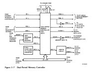
It is indeed real memory. But it is also a dual-ported shared memory. The 82586 ethernet controller has all its buffers and control structure in this space.
 
Hm. That's interesting. I wonder how the OS accesses it, normally you put the buffers over in pool space, not in random places in memory. Next time I boot it I'll check and see what/how it allocates memory in RMD.

From what I can see there was support in 3.2 to set up a Pro as a network server and run diskless Pro/350's. Not sure if it would work, but if we can reverse engineer what files are needed it would be fun to have a 350 boot off my pdp11/83. As it is, it was possible to mount volumes exported on the 11/83 on the 380 which really simplifies data transfers....

Maybe I'll pull the hard drive, put a network analyzer on the ethernet segment and see if it squawks during the boot process.
 
There were actually four cards. I got one of them, but unfortunately it is not working in my 380.
Really? How does it fail, and is it bombing the same way this one does?

There might be a relationship. And if the board is physically the same as mine there might be either a blown chip or bad ROM code sinking them.
 
Really? How does it fail, and is it bombing the same way this one does?

There might be a relationship. And if the board is physically the same as mine there might be either a blown chip or bad ROM code sinking them.
I bought one of the four available. I only have the one DECNA card, and it fails. I believe there were two other buyers, one who may have purchased two cards.
 
That sounds interesting. How do you request a PRO to boot from the network?
It was a while ago when I did this, but IIRC you just set up one Pro as a "server" and IIRC you have to type in the MAC address of the client that will boot (using the "Workstation Registration" app).
Then you just connect them together and turn on the diskless machine. I believe if it has no other boot medium it will just try to boot the network. Assuming your DECNA is working, which seems to be a big assumption.
There is also a "PRONVR" diskette (the "NVR MODIFICATION UTILITY" BL-HD10B-BH available as PRO177-5 thoughtfully mirrored here: https://oldcomputers.dyndns.org/public/pub/mirror/os2site/sw/dec/pro/pro177/177-5.lzh).
Ever wonder what the 50 bytes of battery-backed-up-RAM are for? It turns out some of it stores boot information. With that diskette you can override the default boot configuration so your machine boots from the network even if you have a local hard disk. And IIRC you still have access to the local disk.
It's all pretty darn cool.
I even created a little network with a real PRO with a DECNA and a little Linux box running simh/VAX/VMS and I was able to see the VMS files and 'SET HOST' from the PRO to the VAX. Sadly I couldn't figure out how to get network booting to work from the simh/VAX/VMS system. But file sharing, "CHAT", and remote login all worked fine.
 
Oh, I thought a second person chimed in on the thread. Let us know how the new chips go, I'd really like to have someone else with a working card.
 
Oh, I thought a second person chimed in on the thread. Let us know how the new chips go, I'd really like to have someone else with a working card.
So I ordered a batch of chips. Any guidance on how best to remove them from the board. I was thinking about hot air with a heat gun. I think you also suggested just cutting the chip leads and removing one at a time.
 
I worked my way through the code and it seems to be doing exactly what davibear said for Test 2, writing 0xAAAA, checking the pattern and doing the same with 0x5555 (I did not fully verify). Code 10 looks like a memory problem. I can replace all DRAM chips, but I was wondering if I could write a program to write and read the memory myself to see what bit(s) are failing and then replace those chips. Can I reach the card if it fails the diag test and I continue or is it somehow disabled? I would need to set the PARs, but I believe one of the PARs is already set for physical address 0o1400000, no? Is it possible the 8207 Dual Port DRAM Controller is bad and not the memory itself? If I write a program and see a bit or two, I know it is a memory chip and could locate the chip(s). If many or all of the bits are wrong, then I might assume the 8207.

Here's what I got (maybe not completely correct):

3776: MOV #30,6(R5) ; Start testing DRAM
4004: MOV #203,2056
4012: MOV 2056,4(R5)
4020: MOV #4,-(SP)
4024: MOV #600,-(SP)
4030: EMT 5 ; Save and set PAR registers
4032: MOV #125252,R0 ; Octal #125252 is 0xAAAA
4036: MOV #20000,R1 ; Octal #20000 is 8K
4042: MOV #40000,R2 ; Octal #40000 is 16K counter
4046: MOV R0,(R1)+ ; Write the value and increment the address
4050: SOB R2,4046 ; Loop to write all of the 8KW block
4052: MOV #4,2(SP) ; Sets the parameters on the stack for EMT mapping operation, this one being the number of 8K pages to map
4060: ADD #4,(SP) ; High 9 bytes of physical address
4064: CMP (SP),#614 ; Octal 14 is decimal 12
4070: BGT 4076 ; Finished 0xAAAA write, now go to read back and compare to original value and complement 0x5555
4072: EMT 6 ; Restore PAR registers
4074: BR 4030 ; Jump back to set new PAR registers and write more memory
4076: MOV #40000,R2 ; Reset counter in R2
4102: MOV #52525,R3 ; Octal #52525 is 0x5555
4106: SUB #4,(SP)
4112: BR 4126
4114: MOV #120000,R1
4120: MOV #40000,R2
4124: EMT 5
4126: CMP -(R1),R0 ; Read back the memory to see if has the value it wrote with R0 (0xAAAA), starting at the high memory and coming back down
4130: BNE 4254 ; Failure - Jump to restore PARs and return from subroutine that started 3776
4132: COM (R1) ; Complement the R1 value of 0xAAAA
4134: CMP (R1),R3 ; Compare it to R3 value 0x5555
4136: BNE 4254 ; Failure - Jump to restore PARs and return from subroutine that started 3776
4140: SOB R2,4126 ; Loop back and compare more memory
4142: INCB 2064 ; Increment error code for next block of memory
4146: MOV #4,2(SP)
4154: SUB #4,(SP)
4160: CMP (SP),#600 ; Have we come all the way back down?
4164: BLT 4172 ; Yes, move onto next test
4166: EMT 6
4170: BR 4114 ; No, branch back and continue
4172: MOV #200,2076 ; Moving on
4200: MOV 2100,R0
 
Last edited:
Chip leads clipped. Use a really sharp nipper to minimize stress on the board. Flux is your friend, put it on first and use zephlux. But if possible see if you can figure out what diag is flunking first.
 
I did have a simple thought: it's possible the problem is not the RAM at all.
I believe the RAM tests are the first thing that make use of the high byte data lane. The low bits are probably okay, at least for reading, given that you're able to read the entire ROM (byte by byte) without issue.
Maybe you have a bad bus transceiver in the high data byte?
And yes, maybe the DPRAM controller is bad.
Schematics would be really, really nice (anyone out there have them??)
Yes, you can absolutely write a standalone program to test the RAM yourself.
And yes the board is accessible. You can read/write its registers in the CTI slot it's assigned to, even if it failed diagnostics, then you can tell it to map itself at some physical address and then set up your PAR/PDRs to give you virtual address access to it.
I believe on completion of the boot-time diagnostics, on success or failure, it will remove itself from the physical addressing space, so you'll need to remap it yourself.
For some of my testing what I made a cable that turned on the "maintenance mode" (a cable that shorts pin 9 to ground).
This allowed me to send a break over the serial line to put the machine into ODT mode.
Then I wrote some Python code to download little bits of code directly into RAM. The code would run and report results over the serial port.
This is how I examined some of the functionality on the DECNA when I was writing my emulator.
Most useful for you would probably be exp04.mac. This program finds the DECNA board, maps the DECNA DP RAM and writes to it.
It's been several years, so my memory is a little rusty, but you're welcome to this stuff. I'm skipping the Python code because it is really tied to the terminal emulator I was using (SecureCRT).
BTW you might try Jörg Hoppe's PDP11GUI (https://www.retrocmp.com/tools/pdp11gui) to talk to the serial port. I think I got it to work with my PRO (I can't remember if I was using the 350 or the 380). I do remember it required me to pull some RS-232 signal up to get it to work at all (was it DTR?). But if you got that going you'd be able to download code over the serial port.
--Bjoren
 

Attachments

  • decna_exp.zip
    16.3 KB · Views: 1
I worked my way through the code and it seems to be doing exactly what davibear said for Test 2, writing 0xAAAA, checking the pattern and doing the same with 0x5555 (I did not fully verify). Code 10 looks like a memory problem. I can replace all DRAM chips, but I was wondering if I could write a program to write and read the memory myself to see what bit(s) are failing and then replace those chips. Can I reach the card if it fails the diag test and I continue or is it somehow disabled? I would need to set the PARs, but I believe one of the PARs is already set for physical address 0o1400000, no? Is it possible the 8207 Dual Port DRAM Controller is bad and not the memory itself? If I write a program and see a bit or two, I know it is a memory chip and could locate the chip(s). If many or all of the bits are wrong, then I might assume the 8207.

You should be able to rip out parts of the diagnostic that sets up mapping. I think the PAR is restored back using EMT 6 after the test is concluded. But if you just call EMT 5 with proper parameter you should have you mapping set up. Somewhere you need to write to the base register in the DECNA and then enable the RAM in the DECNA CSR. Potentially all/most of this can be done by hand in the micro-ODT at the console on the printerport. You could even peek/poke memory locations from micro-ODT dosing hand testing as soon as the mapping is set up and board memory is enabled.

I think (but I am not sure) that these lines sets up the DECNA card onboard memory:

3776: MOV #30,6(R5) ; Start testing DRAM
4004: MOV #203,2056
4012: MOV 2056,4(R5)


I find it more likely a DRAM has failed than the 8207, but you are right, if all bits has failed it is probably a 8207 problem (or data bus driver) than a RAM chip failure.
 
Last edited:
It was a while ago when I did this, but IIRC you just set up one Pro as a "server" and IIRC you have to type in the MAC address of the client that will boot (using the "Workstation Registration" app).
Then you just connect them together and turn on the diskless machine. I believe if it has no other boot medium it will just try to boot the network. Assuming your DECNA is working, which seems to be a big assumption.
There is also a "PRONVR" diskette (the "NVR MODIFICATION UTILITY" BL-HD10B-BH available as PRO177-5 thoughtfully mirrored here: https://oldcomputers.dyndns.org/public/pub/mirror/os2site/sw/dec/pro/pro177/177-5.lzh).
Ever wonder what the 50 bytes of battery-backed-up-RAM are for? It turns out some of it stores boot information. With that diskette you can override the default boot configuration so your machine boots from the network even if you have a local hard disk. And IIRC you still have access to the local disk.
It's all pretty darn cool.
I even created a little network with a real PRO with a DECNA and a little Linux box running simh/VAX/VMS and I was able to see the VMS files and 'SET HOST' from the PRO to the VAX. Sadly I couldn't figure out how to get network booting to work from the simh/VAX/VMS system. But file sharing, "CHAT", and remote login all worked fine.
Thanks!
 
Both of you are spot on. I was loupe'ing the board last night to look for open solder joints and other physical failures. As a general note, the soldering quality on these boards with the silver traces doesn't seem to be as good as the boards with the green coating. There are pits and gaps, but not so bad as to cause an open circuit. I started to reverse engineer the traces to figure out how the memory connects to tri-state buffers, Octal D latches and the 8207. I started questioning whether it is the memory, 8207 or other logic. I presume a pass on Test group 1 suggests the 8207 is working at least partially, or am I wrong there? I am not sure the ROM is behind the 8207, so I might be able to read the ROM, but not get to the DRAM. I assume the ROM needs to be read before setting up the 8207. I'm familiar with ODT mode and have a cable and notes from using it in the past. Yes, short the pin, send the break. I was able to do it with Putty on a laptop. Davibear's code will be a tremendous help to reduce debugging new test code. I need to look at the code to see what's more efficient, typing in via ODT or running a program from the toolkit. I have not been successful in locating any schematics for the DECNA card. The board is not that complex to manually trace it out if we want to go there. But this is great. What a wealth of knowledge that I did not know existed. Thank you.
 
Last edited:
No the ROM is not behind the 8207. The 8207 only handles DRAMs. I.e. it has row/column multiplexing logic and refresh management. There is a simple counter that addresses the ROM and each time you read from baseport+0 you get the current data from the ROM and the counter is incremented. Then if your write to baseport+2 the counter is reset.

I think you are on the right path here using the assembly snippets that davibear provided together with some ODT console hacking and you will quickly find out what bit or addresses that are failing. Good luck!

Since DECNA is such a scarce resource I have a vague idea of creating a replica. Basically replacing most of the logic with programmable logic. The DRAM is then replaced with an SRAM chip. I will keep the 82586 which I can harvest from some old PC network boards I have. Actually there are chips on Ebay. With all the good info that davibear have provided it will now be much much easier to do this project. However if you find time to trace out your card it can be helpful for such a project. For example I am curious how the ~XACKA output from the 8207 is connected. This signal is inverted so it passes through an inverter, perhaps a 7404 and then ends up at pin 37 ARDY on the 82586. It would be great if you have time to trace this signal back from the 82586 to the 8207!
 
Yes, I am of the same opinion about replicating the card. I think we have enough information and knowledge with this team to make it feasible. It took me a long time to find a card, and of course, the only I received did not work. I'll check into ~XACKA trace routing this evening.
 
No the ROM is not behind the 8207. The 8207 only handles DRAMs. I.e. it has row/column multiplexing logic and refresh management. There is a simple counter that addresses the ROM and each time you read from baseport+0 you get the current data from the ROM and the counter is incremented. Then if your write to baseport+2 the counter is reset.

I think you are on the right path here using the assembly snippets that davibear provided together with some ODT console hacking and you will quickly find out what bit or addresses that are failing. Good luck!

Since DECNA is such a scarce resource I have a vague idea of creating a replica. Basically replacing most of the logic with programmable logic. The DRAM is then replaced with an SRAM chip. I will keep the 82586 which I can harvest from some old PC network boards I have. Actually there are chips on Ebay. With all the good info that davibear have provided it will now be much much easier to do this project. However if you find time to trace out your card it can be helpful for such a project. For example I am curious how the ~XACKA output from the 8207 is connected. This signal is inverted so it passes through an inverter, perhaps a 7404 and then ends up at pin 37 ARDY on the 82586. It would be great if you have time to trace this signal back from the 82586 to the 8207!
That would be a great project. I proactively picked up a handful of the bus connectors with something of this sort in mind.
 
I am curious how the ~XACKA output from the 8207 is connected. This signal is inverted so it passes through an inverter, perhaps a 7404 and then ends up at pin 37 ARDY on the 82586. It would be great if you have time to trace this signal back from the 82586 to the 8207!
Pin 37 ARDY/SRDY is on the right of the 82586 in the middle of the chip just above VCC (Pin 36). Pin 37 is an input and it has a hard ground. I confirmed Pin 36 is VCC.
~XACKA is pin 2 on the 8207. It connects to pin 11 (enable input) on a 74LS373 in the same column (E50) as the 8207, third chip down from the top.
 
Thanks for checking this. Obviously I mixed things up.

Screenshot 2024-04-18 at 06.53.00.png

It says in the tech manual that XACKA L goes to the CTI memory Data latch so it is indeed exactly what you have written. What I wanted you to check was to check where the AACKBL (5) signal goes. It should go through a 7404 and then to the 82586. Since the ARDY/SRDY is grounded then it has to go to the READY (39) input. Sorry for the confusion.
 
It says in the tech manual that XACKA L goes to the CTI memory Data latch so it is indeed exactly what you have written. What I wanted you to check was to check where the AACKBL (5) signal goes. It should go through a 7404 and then to the 82586. Since the ARDY/SRDY is grounded then it has to go to the READY (39) input. Sorry for the confusion.
Confirmed. AACKBL (5) signal goes to pin 13 on the 7404. Pin 12 output goes to READY (39) on the 82586.
 
Thanks! I wonder how the BRPLYL signal is generated on the CTI bus. Surely a ACK / READY signal from the 8207 has to be involved somehow. A CTI RAM access may be stalled since the 82586 is accessing the RAM and then the CTI bus transaction has to wait. Is the signal AACKAL used somehow to generate BRPLYL? It is not mentioned in the picture above unfortunately. If you have time you maybe can see if you can trace BRPLYL backwards a bit to see if it has to do with XACKAL? BRPLY can be quite complex since there are many sources for BRPLYL signal as far as I can understand.
 
Back
Top