• Please review our updated Terms and Rules here

41256 DRAM Tester

8008guy

Veteran Member
Joined
Jun 25, 2014
Messages
584
Location
Salt Lake City, Utah
I threw this DRAM tester together today. It's for 41256 DRAMS, although it should work for 4164's as well. It's based on a bread-boaded Arduino UNO. (ATMEGA 328P) It runs four different test loops, all zeros, all ones, alternate 0's and ones and then alternate 1's and zeros. Three LED's will indicate the status, and then it will continue to loop. There is a serial port in the design, I use it for uploading the program. But it could be used to print out info as the program runs.

Schematic and Source at this link:

http://www.chronworks.com/DRAM/

I tested this with a 41256 and it runs fine. I watched all the signals on a logic analyzer and the timing appears to be good.

The only things that I'm not quite clear on is the refresh cycle. The chip specs out a 4ms refresh cycle. My RAS loop takes around 14ms to cover 0 to 511 rows. Am I understanding the data sheet correctly? Or am I covering the refresh ok? All the tests complete with no failures.

If anyone has a compelling reason why this is running too slowly I can jettison the Arduino environment and just do straight AVR, though without trying it I'm not sure how much I will gain. Anyway... I am rambling at this point. :bigups:

I'm going to find some 4164's to test as well.

Please play around with it. If you make it better let me know so I can update the project files.

len
 
The only things that I'm not quite clear on is the refresh cycle. The chip specs out a 4ms refresh cycle. My RAS loop takes around 14ms to cover 0 to 511 rows. Am I understanding the data sheet correctly? Or am I covering the refresh ok?
To the outside world, there appears to be 512 rows and 512 columns, because a motherboard (or whatever) presents a 9-bit row to the chip and then presents a 9-bit column.

But, if you look at the 41256 specs/datasheets at [here], you will see that 41256-class chips have a cell matrix of 256 rows by 1024 columns, not the 512 rows by 512 columns that you would expect.
The 512x512 row/column address presented to the chip is internally converted to 256x1024 for the cell matrix. A diagram showing that is on the second page of the Austin AS4C1259 datasheet; note that one of the row address bits is diverted to the column decoder (becomes an extra column address bit).

The internal 256x1024 cell matrix is why the 41256 datasheets indicate that only 256 rows need to be addressed within the specified refresh period.

So your code's RAS loop of about 14 ms, covering 512 rows, is actually addressing all of the 41256's internal rows (quantity of 256) twice.
So your "about 14 ms", from the 41256's perspective, is actually "about 7 ms".
Still, 7 ms is a long way off the 4 ms spec.
 
Something that you should be aware of is a start up requirement of these chips. The following text are samples from only four datasheets.

"An initial pause of 200 uS is required after power-up followed by any 8 RAS cycles before proper operation is achieved."

"8 cycles are required after power-on or prolonged periods (greater than 2 ms) of RAS inactivity before proper device operation is achieved. Any 8 cycles which perform refresh are adequate for this purpose."

"An initial pause of 100 us is required after power-up followed by any eight RAS cycles before proper operation is assured. The eight RAS cycle wake-up should be repeated any time the refresh requirement is exceeded."

"An initial pause of 100 uS is required after power-up followed by 8 initialization cycles before proper device operation is assured. 8 initialization cycles are also required after any 4 ms period in which there are no RAS cycles. An initialization cycle is any cycle in which RAS is cycled."

The figure of 8 for 'RAS required before proper operation' is consistent.

And so if you experience data read problems, it could be because the above is not being met. Maybe you should add 8 dummy reads before any testing.
 
Thanks guys, all good comments.

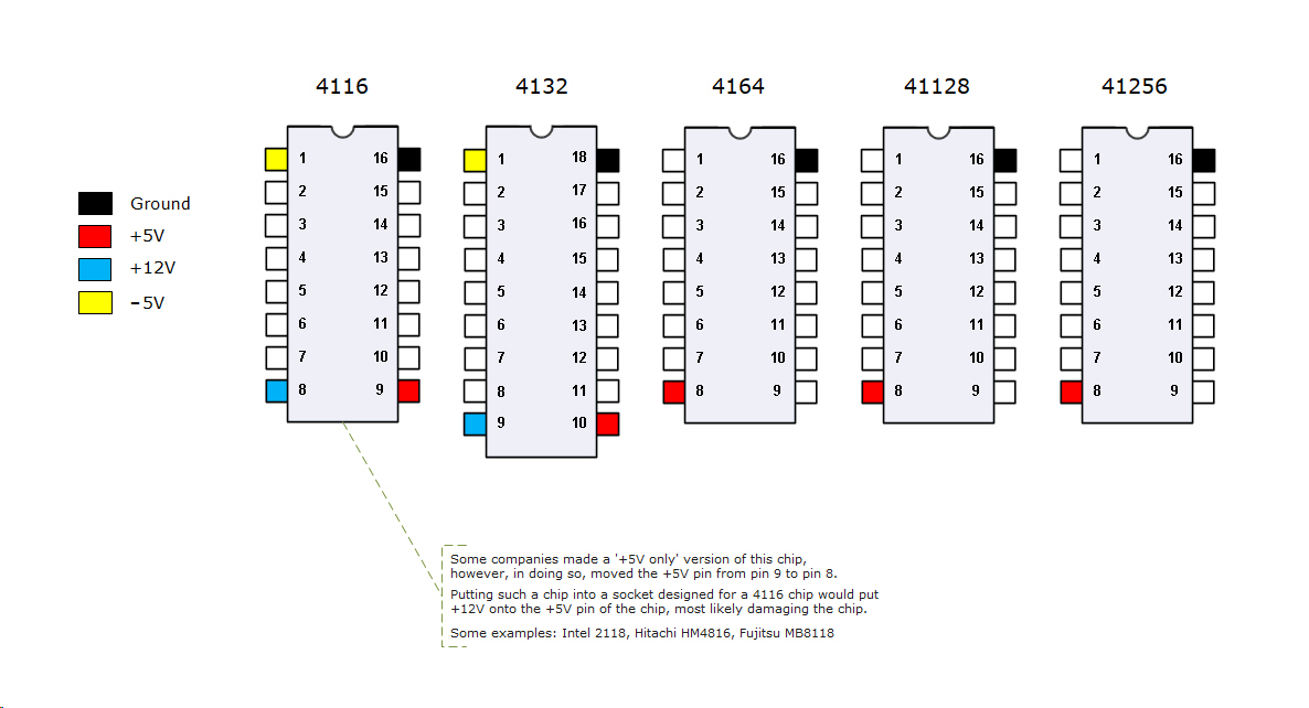
Funny, I caught the reversed power pins when I was comparing the data sheet of the 4164. I never powered up a chip thankfully before I realized that.

I'm working on a straight AVR implementation with a larger chip. Hopefully I can get things tighter with more io pins.

len
 
Funny, I caught the reversed power pins when I was comparing the data sheet of the 4164. I never powered up a chip thankfully before I realized that.
In case it is of any use:

4116_4164_41128_41256_power.jpg
 
Back
Top