• Please review our updated Terms and Rules here

A MC68340 homebrew

Plasmo

Experienced Member
Joined
Aug 29, 2017
Messages
307
Location
New Mexico, USA
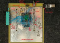
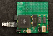
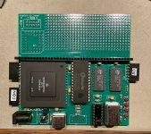
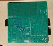
MC68340 is a member of CPU32 family which are microcontrollers based on MC68000 core. I bought several tubes of surplus MC68340 20+ years ago and built up a prototype board to check it out and then forgot about it. My interest is rekindled by recent discussion about “mc68340-cpu32-looking-for-the-answers” and managed to find the 68340 prototype board. I've made further progress with the prototype adding a boot ROM, IO clock and serial port interface; I've ported a simple monitor and ported TUTOR v1.3 to the prototype board; and I've designed a pc board version which should arrive in a week. Before putting away the prototype board (like the last scene of “Raider of Lost Ark”), I'm documenting what I did with this prototype as well as future progress with the pc board version.
 

Attachments

Received SBC68340 pc board from JLCPCB and built one up. The main difference between prototype 68340 and SBC68340 is the port size of RAM which has changed from 8-bit to 16-bit for SBC68340. This change requires a change in CS1 base register initialization and different hardware decoding logic for upper RAM and lower RAM. I was not happy with the reference design of decoding logic in Motorola 68340 user manual so I designed a simpler version based on a 7486 exclusive-OR gate. Just in case my design is wrong, I have a backup CPLD in the prototype area of the board. It turns out the exclusive-OR decode works, so CPLD is not needed. The 7486 is in the critical decoding path so I've designed with 74ACT86, but I have not received it so I tried the standard TTL 7486 which appeared to work at 24MHz zero wait state.

The prototype monitor software and TUTOR v1.3 (posted in previous post) worked once the RAM port size is initialized to 16-bit.

I plan to implement bit-bang SD card interface and port CP/M68K.

Having an uncommitted CPLD and a breadboard area will give me room to experiment.
Bill
 

Attachments

Nice work.

I assume that the configuration for the ROM (/CS0) has also been changed to a base address of $40000 to account for the two (2) 128KB RAMs?

I further assume that /DSACK0 is only used by the CPU bootstrap mode - judging by the configuration of the /CS0 registers?

I see that the 340bug code contains a Compact Flash CP/M 68K bootstrap, and that connector P6 seems to have sufficient signals on it to support a Compact Flash card in 8-bit IDE mode. It is (perhaps) a shame that D0..D7 has been routed to P6 instead of D8..D15. I assume this was intentional?

/CS3 appears to be routed to P6 so (on the assumption that the CF card is fast enough - or the CPU clock is slow enough) that this could be used (with a bit of tweaking to the 340bug code) to boot CP/M 68K?

Dave
 
Thanks for reviewing. You right about changing CS0 to $40000 to accommodate larger RAM. While DTACK0 is driven by CS0 directly, I plan to add a schottky diode to isolate it from P6. P6 was thrown in last moment to provide test points for logic analyzer; the data lines ought to be D[15…8]. Thanks for pointing it out. P6 pin assignments are similar to RC2014 bus, so RC2014-compatible CF board may be used with minor reworks. Most of my 68K designs used CF interface, so there are remnants of CF interface in the monitor code. In this design I’m shooting for a simple baseline design to reach CP/M 68K capability, so I’m exploring bit-bang SD card interface using 68340’s discrete IO. It’ll be slower than CF for sure. The main purpose of rev0 board is making sure I have created the 68340 library correctly, checking out the 16-bit RAM decoding logic, and having a low-insertion force PGA socket to check out the batch of 68340 I have on hand.
Bill
 
I should have checked the RC2014 bus specification. I thought the physical footprint looked familiar!

I see you are using the SN7486. The bell in my brain went off! Then I remembered what it was - the SN74L86 has a different pinout. That is OK, the 'L' part will be too slow anyhow...

I am slowly working on an interesting project with a 68000 CPU. It is an 8-port terminal server with plenty of RAM, ROM and an ETHERNET interface. It doesn't have a means of storage though - so I am thinking about bit-banging one of the terminal handshake lines with an interconnected SD card. Slow, but it should be workable... I want to get a simple monitor, TUTOR and CP/M 68K running on that. I have the schematics, but I am slowly working out how the beast works. It is 'interesting' because it uses DRAM and performs the refresh with the CPU via a high-priority timer interrupt. DRAM is at location 0 (once the memory map has been manipulated to move the EPROM and map in the DRAM) so we use an interrupt vector (in DRAM) that I have to refresh to maintain its contents. I see crashes ahead when I get around to writing the firmware for it! But that is half the fun isn't it!

Dave
 
Last edited:
This is the gerber photo plots for SBC68340. It is 2-layer pcb, 4”x4” which should be $2 for 5 boards from JLCPCB plus whatever shipping charge.

My earliest retro 68000 (circa 2017) had 16 meg DRAM starting from $0. On reset, a state machine kept 68000 in reset, took over DRAM multiplexed address bus and loaded 32K of data from serial EEPROM into DRAM. I did CAS-before-RAS refresh when Address Strobe is negated every 16uS. I was worried about memory not being refreshed when rebooting after program has crashed thus losing memory contents leading to the program crash, but I have found the DRAM refresh timing is extremely conservative at room temperature. Memory contents are good for several seconds without refresh. That characteristic was very helpful during debugging.
Bill
 

Attachments

PCBs ordered just now.

On the assumption everything works with the order - I will have four (4) PCBs spare if anyone wants one in the UK.

Dave
 
I have created a homepage for rev0 of SBC68340 here:
I will add all the hardware and software design information there. It will also include experimental projects with SBC68340 which may need cuts, jumpers and additional components in the prototype area.

To make sure the design is repeatable and to accommodate RC2014 expansion boards (CF disk, VGARC), I built second board with RC2014 connector installed and significant modifications to RC2014 expansion bus. The second board works.
Bill
 

Attachments

  • IMG_5475.jpeg
    IMG_5475.jpeg
    2.1 MB · Views: 4
  • IMG_5476.jpeg
    IMG_5476.jpeg
    1.7 MB · Views: 4
Just ordered the RAM, PGA socket and CPU (I can only find a 16 MHz part - so I will replace the crystal oscillator accordingly).

What is the full part number for the MCP130D? This is a generic part (130 = internal 5k pull-up resistor, D = TO-92 'D' pinout). But there should be another number on the end identifying the low voltage limit (not that it is probably significant though).

The other question I had is regarding the oscillator modules. Some have an enable/disable pin and others not (normally pin 1). Have you connected this pin on the PCB or not? The crystal oscillator modules I have found so far have the enable/disable pin. Happy to add a wire of course...

Dave
 
It is MCP130-450DI/TO.

Pin 1 of can oscillator is floating (unconnected). I probably have 20 different can oscillators, none of them has enable input.
Bill
 
Cheers for the part number.

I guessed so with the oscillator (because your schematic did not show it). I thought I would ask the dumb question though...

Dave
 
I think I have a working CP/M-68K for SBC68340.

SBC68340 does not have much memory; it has 64KB flash and 256KB RAM. To install CP/M-68K, I put CPM15000 in memory $15000-$1AFFF and BIOS from $1B000-$1BFFF. TPA for CP/M starts from $20000-$3FFFF for 128K of TPA. The 64KB flash has top 32K free for a small ROM disk which is enough for 3 programs: init.68k, pip.68k, and stat.68k. Since CP/M-68K starts from $15000, there are free RAM memory from $400-$14FFF. I created a small 64KB RAM disk starting from $1000.

The BIOS is a pared down version of MPU302 BIOS. I load S-record of BIOS and CPM15000 via serial port into memory and then run from $15000: I got a CP/M-68K prompt; with 'dir' command I can see the 3 programs in flash drive; I can initialize RAM drive B with 'init b:' command; I can pip with verify from drive A to drive B; switching to drive B, I can see the 3 newly copied program with 'dir' command; and I can do 'stat *.*' of drive B and see file attributes of the 3 programs.

Attached is screen shot of the session.

Now I need to work on interface to SD card for mass storage.
Bill
 

Attachments

  • cpm68k_on_SBC68340.jpg
    cpm68k_on_SBC68340.jpg
    106 KB · Views: 3
Nice.

I have my 'bits' arriving slowly.

The PCB has been manufactured and is on the way.

The CPU, CPU socket, RAM and crystal oscillator modules have just arrived.

I will do a large parts buy from a local UK supplier when the PCB arrives.

The pins on the RAM are small! I will start with soldering the RAMs I think - just in case I make a mess of it!

Dave
 
Back
Top