• Please review our updated Terms and Rules here

A225 Deflection Amplifier PCB

thunter0512

Veteran Member
Joined
Sep 27, 2020
Messages
859
Location
Perth in Western Australia
Has anyone got a more readable scan of the A225 Deflection Amplifier PCB than what is shown on page 15 of:

http://www.bitsavers.org/pdf/dec/graphics/VT11/VR17_Engineering_Drawings_Mar75.pdf

The schematic on the following page is a poor print or scan too, but I found a few alternatives.

Here is the page from the manual above:
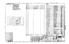
A225 PCB.png

Could anyone with a better scan of that (or similar) page please make it available?

Thanks
Tom
 
Last edited:
That scan seems quite typical of many DEC schematics from that era. What area of the schematic (or info) are you having difficulty with?
 
Even original schematics are hard to read sometimes,have some hardcopies of org. PDP8M and several of those schematics even vage.
You have to be creative as comparing with real hardware, component listings, pcb drawings, datasheets to figure out.
Also lot of schematics are scanned way back when limit of data storage and out of date scanners,yellowed pages converted to B&W.
Buy original manual and start new scan and make it available.
 
I am struggling to read some of the component designations and values.
Purchasing an original manual with a better quality schematic and component designations seems highly unlikely.
... just guessing which component designations might be difficult to decipher. ex:

A225-th.png

Please to refer to p. 25 and p. 346 of the DEC Component Index to see if you agree with my interpretations.
 
I've started to update
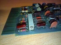
and it's interesting that the photo shows C17 is not installed. This is probably related to "Note 3" and the little table upper right of the component location diagram.

Vince
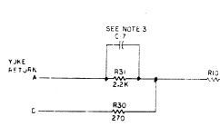
Thanks Vince. I have C17 (100 pF) and parallel to it R31 (2.2k) as shown in the VR17 Engineering Drawing. The capacitor exists only in the YB variant and can be from zero to 180 pF. There are several ECOs for the A225 dealing with this capacitor issue and the YB variant of the A225 which was meant to be used in the GT40.

Your photo shows that the optional C17 is not fitted, but confusingly R31 (or R33 in later schematics) is not fitted either. I don't think this resistor can be optional as it means that "yoke return" on pin A is open circuit. Of course there is the mysterious pin D input which has R30 a 270 Ohm resistor connected to the right hand side of where C17 connects, so it may be that in some configurations pin D is used instead.

1665313411411.png

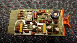
Here is a photo of mine showing C17 parallel to R31 in the bottom left of the populated area of the PCB:

IMG_20221009_183814128.jpg
 
Here is a photo of mine showing C17 parallel to R31 in the bottom left of the populated area of the PCB:
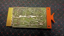
I think Dave's board (the photos are derived from ones on his website) is a newer revision, and R31 mounts in the adjacent pair of holes. The two sites can be seen to be connected in parallel in A225Eback.jpg.

Vince
 
Hmmm - just noticed on the photo that R17 is badly burned. It is meant to be 75 Ohm but is now 62 Ohms.
Curious that I didn't notice this before. It might mean that it burned during my final testing.
 
Back
Top