bradr
Member
Hey All,
I thought I'd share some info on a project I've been working on - it's yet another FPGA implementation of a TRS-80 that I started as a holiday hacking project over the Christmas break. Although the main goal of this project was to improve my FPGA development skills, it's turned our pretty well and I think worth sharing. My original target for this was to implement just enough of a TRS-80 Model 1 to be able to load games from cassette and play them - which it can do, but I'm now thinking about extending it.
Here it is in action with my son playing Defense Command using a Playstation controller that's emulating a TrisStick.
So far it implements a TRS80 Model 1 with Level II BASIC and 48k RAM. It's implemented on a Mimas V2 FPGA development board which is an almost perfect board for project's like this (I did a review of it here).
Video controller output is via standard VGA connector and supports green or amber screen, and optional scan line emulation (see here). Output is 800x600 with correct TRS-80 2:3 aspect ratio for pixels.
Keyboard input uses a PS2 keyboard via a PMod connector to the Mimas and can work in either topographical mode (where keys match the approximate position on the TRS-80 keyboard) or typing mode (where characters are remapped to make using a PC keyboard seem normal eg: Shift+2 gives an @ symbol unlike TRS-80).
It supports loading .cas files from an SD card and renders the raw bytes from the .cas file to an audio stream which is fed to the TRS-80's cassette input. Similarly for recording the FPGA hardware parses the generated audio stream and writes the raw bytes to the SD card in .cas file format. Currently the SD card needs to be specially formatted with a custom file-system where each file is numbered and the tape image is selected by using the buttons on the FPGA board and the selected tape is shown on the 7-segment display. This is less than convenient but I have plans to improve it (see below).
Since the CPU core and the cassette render/parsing logic is all driven from the same clock, I can overclock everything while loading and saving and get a "turbo tape mode" which reduces a 3+ minute load to about 8 seconds. This overclocking happens automatically when the cassette motor relay is turned on - so it's pretty seamless: the tape loads in turbo mode and then things revert to normal speed.
I've also implemented an auto-cassette mode the detects when cassette record or play operation starts (it tells the difference by monitoring port I/O activity) and automatically starts the virtual cassette recorder - so you don't need to manually start it yourself. See here for turbo mode, recording and auto start/stop demo.
That's what's currently implemented but I'm now working on some improvements. The biggest pain with it in it's current state is the need for a specially formatted SD card and it would be much easier if it could be FAT formatted as this would make copying .cas files to/from it much easier. Implementing FAT support in FPGA logic isn't feasible but there's a couple of options that I've considered:
1. Run the FAT/SD support on a separate microcontroller
2. Run a second soft-core processor on the FPGA and have it perform the FAT work.
I don't like the idea of a separate microcontroller because I'd prefer keep it all on the one board. A second processor is probably doable but I'd prefer not waste the space on the FPGA so instead I've decided to hijack the TRS-80's Z80 via NMI and switch to a separate address space and run all "system control" functions there. I've got a basic proof of concept for this working but still a lot of work to do.
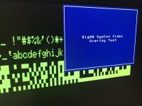
This system control software (aka syscon) will also need a UI so I've also implemented a simple 32x16 character video overlay that will be used to select tapes and eventually disk images:

Anyway, it's been a fun project so far. If you're interested, source code and operating instructions are available here:
https://github.com/toptensoftware/big80
and more in-depth articles here:
https://www.toptensoftware.com/blog/tag/big80/
Interested in feedback
Brad
I thought I'd share some info on a project I've been working on - it's yet another FPGA implementation of a TRS-80 that I started as a holiday hacking project over the Christmas break. Although the main goal of this project was to improve my FPGA development skills, it's turned our pretty well and I think worth sharing. My original target for this was to implement just enough of a TRS-80 Model 1 to be able to load games from cassette and play them - which it can do, but I'm now thinking about extending it.
Here it is in action with my son playing Defense Command using a Playstation controller that's emulating a TrisStick.
So far it implements a TRS80 Model 1 with Level II BASIC and 48k RAM. It's implemented on a Mimas V2 FPGA development board which is an almost perfect board for project's like this (I did a review of it here).
Video controller output is via standard VGA connector and supports green or amber screen, and optional scan line emulation (see here). Output is 800x600 with correct TRS-80 2:3 aspect ratio for pixels.
Keyboard input uses a PS2 keyboard via a PMod connector to the Mimas and can work in either topographical mode (where keys match the approximate position on the TRS-80 keyboard) or typing mode (where characters are remapped to make using a PC keyboard seem normal eg: Shift+2 gives an @ symbol unlike TRS-80).
It supports loading .cas files from an SD card and renders the raw bytes from the .cas file to an audio stream which is fed to the TRS-80's cassette input. Similarly for recording the FPGA hardware parses the generated audio stream and writes the raw bytes to the SD card in .cas file format. Currently the SD card needs to be specially formatted with a custom file-system where each file is numbered and the tape image is selected by using the buttons on the FPGA board and the selected tape is shown on the 7-segment display. This is less than convenient but I have plans to improve it (see below).
Since the CPU core and the cassette render/parsing logic is all driven from the same clock, I can overclock everything while loading and saving and get a "turbo tape mode" which reduces a 3+ minute load to about 8 seconds. This overclocking happens automatically when the cassette motor relay is turned on - so it's pretty seamless: the tape loads in turbo mode and then things revert to normal speed.
I've also implemented an auto-cassette mode the detects when cassette record or play operation starts (it tells the difference by monitoring port I/O activity) and automatically starts the virtual cassette recorder - so you don't need to manually start it yourself. See here for turbo mode, recording and auto start/stop demo.
That's what's currently implemented but I'm now working on some improvements. The biggest pain with it in it's current state is the need for a specially formatted SD card and it would be much easier if it could be FAT formatted as this would make copying .cas files to/from it much easier. Implementing FAT support in FPGA logic isn't feasible but there's a couple of options that I've considered:
1. Run the FAT/SD support on a separate microcontroller
2. Run a second soft-core processor on the FPGA and have it perform the FAT work.
I don't like the idea of a separate microcontroller because I'd prefer keep it all on the one board. A second processor is probably doable but I'd prefer not waste the space on the FPGA so instead I've decided to hijack the TRS-80's Z80 via NMI and switch to a separate address space and run all "system control" functions there. I've got a basic proof of concept for this working but still a lot of work to do.
This system control software (aka syscon) will also need a UI so I've also implemented a simple 32x16 character video overlay that will be used to select tapes and eventually disk images:

Anyway, it's been a fun project so far. If you're interested, source code and operating instructions are available here:
https://github.com/toptensoftware/big80
and more in-depth articles here:
https://www.toptensoftware.com/blog/tag/big80/
Interested in feedback
Brad
