• Please review our updated Terms and Rules here

Board scans wanted for IBM 5160 cloning project

MadCatSE

Member
Joined
Apr 18, 2024
Messages
11
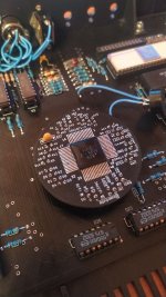
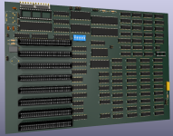
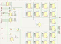
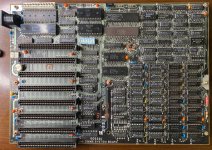
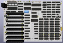
Hello fellow retro computer fans! I want to share my recent project progress and ask for a little help. I have been looking for an IBM PC 5160 for several years, but the prices for them are off the charts where I live, so I kind of gave up on it. Until a couple of weeks ago, when I stumbled upon the recreation project for the original IBM CGA video card by hkzlab. He did a really great job, using original IBM documentation for it. So that got me thinking - how hard could it be to recreate the whole motherboard for XT? I mean IBM did put the complete schematics in its Technical reference, all 10 pages of it. So I decided to do it, and it took me about two weeks to transfer schematics to KiCAD, while creating symbols and footprints, studying datasheets and now it's sort of ready for tracing. And here is where I have a problem. I have some experience with reverse-engineering old boards, with two finished projects (one is a Soviet ZX Spectrum clone, the other is a rather interesting 16-bit ISA controller for archiving data to VHS tapes called "Arvid-1020"), but I had original boards in my possession, so I could test the board for connections and continuity with a multimeter if I wasn't sure if my schematics are correct. But all I have for 5160 are several photos of varying quality, and a recently repaired XT clone that I use for a sanity check of my design. It's hard, but could be done. The second problem is much bigger. I usually place a scanned image of the board on a user layer in KiCAD, so I can use it as a reference of where to place the components. The image must be from a scanner so there are no distortions of perspective and the dimensions are correct and to scale of the whole board. But common photos are bad for it, dimensions are distorted, and I want the board to be as close to the original as possible.

So, this is my cry for help - can anyone who has the original IBM 5160 64-256kb motherboard in their possession scan it's backside with maximum quality and share the scan of it? The project will be available for everyone after testing, and I promise a huge Thanks printed on the backside of the board to all people who will help with it. Contact me on PM if you are interested in helping4.png
 

Attachments

  • 0.png
    0.png
    715.9 KB · Views: 16
  • 3.png
    3.png
    189.3 KB · Views: 15
I mean IBM did put the complete schematics in its Technical reference, all 10 pages of it.
Be aware that there are errors in IBM's documentation for the PC family, and that includes the circuit diagrams. As I was encountering documentation errors, I would add them to [here], but at some point, I pretty much gave up.

Of interest to you may be the PC-Retro, a 5150 motherboard copy. See [here]. As written on that web page, mmruzek (MTM Scientific) found differences between his 5150 motherboard and the documentation. An example is shown at [here].

Be aware of different 64-256KB motherboards. For example, looking at the image in your post #1, there is an IC socket position labelled "SPARE". If you go to [here], the 64-256KB motherboard shown as 'IBM PC 5160 64-256kB System Board #3' has instead, an IC there, designated U90.
 
scan it's backside with maximum quality and share the scan of it?
I know I've got at least one loose board and another in an XT, that are the 64K to 256K variety, I'm not sure if they are the same though. Are you wanting the board placed on a scanner? Or will a photograph work? I don't think my scanner would handle a board that big, and I'm not sure of the quality it would produce with something that is not as flat as a document.
 
Be aware that there are errors in IBM's documentation for the PC family, and that includes the circuit diagrams.
I am very aware of that, and encountered (and fixed) several errors even while entering the design. Thanks for the link, it will come useful! I already knew about the caps (0.047uF instead if 0.047pF in the documentation. What purpose would 47fF serve? Traces themselves have much more parasitic capacity than 47fF. 47nF is another matter.) As for 5150 copy - I know about it and will use it accordingly. Although they have schematics and PCB in some ancient KiCAD format that even old KiCAD 4 would barely load.
For example, looking at the image in your post #1, there is an IC socket position labelled "SPARE"

Yeah, I have no idea what that is for yet. But there are more differences, for example time delay TD2 is changed to a resistor. I plan to test the schematics with my XT clone board. It's somewhat similar to original XT, uses the same chip set (heh, so THAT is where that word came from) and I already successfully used the IBM documentation for repairs on it (one LS373 was dead and shorted A0 to ground).

Are you wanting the board placed on a scanner? Or will a photograph work?
I have photos, but now I need a scanned image. I tested it with my clone board and it BARELY fits on a typical multi-functional scanner from samsung. I need a backside scan, where there is a clear view of mounting holes and vias for traces. With that I can correctly place all elements, and begin tracing. Scanning of the front is useless, it won't have correct focus because of different heights of all the elements. Backside is flat enough.

2024-04-22 21.09.04.jpg
 
I got quite a few boards, but surely -0degrees must have them all ;) Aren't there several revisions? At least some differ by color. The 5150s come in many versions with the different patch cables. Which one are you looking for on the 5160?

Also what region / location are you?
 
I have a lot of photos, yes. But I need scans. Look at the photo of my clone board - can you see how ICs on the top are sort of pointing upwards? The same is true for ICs on the bottom, but they point downwards. That is because of the perspective distortion, made by the lens of the camera. I can use this photo for reference, but I can't use it for placing the components, not unless I somehow fix the distortion. But my skills in Photoshop are... nonexistent. As for which board I look - any board will do, I need it for components placement, and they are mostly the same across all the 5160s.

As for location - it's russia. Thanks to a certain someone (whose departure I certainly won't miss), there is no eBay access for us anymore, and local prices for something like the 5160 are absurd. There is only one machine for sale now, and it's $1000 USD, excluding shipping. Even XT clone boards are kind of expensive; a working one could be around $100 USD. Mine was $20 USD, but it wasn't working and the seller sort of gave me a discount because I told him what that board was for.
 
The board wouldn't quite fit on the scanner I had easy access to, so I scanned it in both directions. My older scanner seems better, and I think it will do longer documents, but it's in storage right now.

They also seem a little fuzzy, perhaps because they cannot sit flat on the glass.
0012_20240502085746_001.jpg0013_20240502085901_001.jpg
 
The board wouldn't quite fit on the scanner I had easy access to, so I scanned it in both directions. My older scanner seems better, and I think it will do longer documents, but it's in storage right now.

They also seem a little fuzzy, perhaps because they cannot sit flat on the glass.
Thank you very much! 🙏I've combined both images and scaled them up by ISA connector (nice and long), and it looks well enough for the time being. Still I would be grateful for full scans if it's not too much hassle.
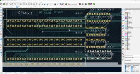
 

Attachments

  • scanned_result.jpg
    scanned_result.jpg
    2.5 MB · Views: 8
Well, it's almost done. I couldn't solve problems with original tracing; it was too much for me. And I'm almost sure that IBM sort of used inner power layers for signals, since I've found strange vias that have a trace to the IC on the top layer and no trace on the bottom layer. I also didn't have enough information about the top layer routing, only the bottom, and I couldn't check anything without having the board. So, after 3 days, I gave up and autotraced the whole board. Vias are too small for original IBM tracing, and traces themselves are 0.25 instead of 0.3, but it's probably okay since there are no high currents and high frequencies. Although maybe I will use Hyperlynx to check signal integrity just to be sure. Power and ground layers are fine. So now I need to re-check everything against the schematics again, and it's probably ready for production.
 

Attachments

  • original.jpg
    original.jpg
    1.1 MB · Views: 11
  • copy.jpg
    copy.jpg
    589.5 KB · Views: 10
How does one do that?
KiCad has a 'FreeRouting' plugin. Actually, I used a standalone version (with exporting of .dsn to it and importing of .ses files back to KiCAD) and sort of abused a server at the university where I work for it to run for a couple of days. It's not perfect by any means and is generally frowned upon by serious PCB designers. But if you know what you're doing, using net classes correctly, setting constraints, feeding those net classes and constraints in the correct sequence to FreeRouting, the result might be quite nice. Well, at least it will work. :)
 
I think this is an interesting project, but I question the cost-effectiveness vs purchasing an original board. Single quantity, large PCBs aren't cheap.
 
but I question the cost-effectiveness vs purchasing an original board
I don't. I would LOVE to purchase the original board, but I can't. The ONLY ONE for sale is in a 1000 USD machine, plus extra for shipping. Being a retro PC fan in russia is suffering. :(

Plus, it's fun to make it, and I can probably sell some spare boards later to recoup some of my losses.
 
I guess that changes things a bit. There are several on US ebay now from $70-$150, but no way for you to get them...

Remember you also have to source all the components, some of which are getting harder to find. The MTM 5150 kits started at $150 but increased to $350 before they were discontinued.
 
I guess that changes things a bit. There are several on US ebay now from $70-$150, but no way for you to get them...

Remember you also have to source all the components, some of which are getting harder to find. The MTM 5150 kits started at $150 but increased to $350 before they were discontinued.
I know, but here is where I'm sort of lucky. The other side of the medal, so to speak.
First of all, I got myself a rather cheap clone board ($20) that I can source components from if necessary (8088 and all accompanying chip set; they all work, and I can test others if I desolder them and install sockets; that's the plan). Secondly, USSR cloned the 8088 in the late '80s and created the K1810VM86 chip, along with all the accompanying ICs for it. They aren't common, but are still somewhat available for $1-2 each. Even 2118 RAM for an IBM CGA card I want to replicate, for example, in the form of a clone K556RU6, costs around 50 US cents each, so a full stack of video RAM is less than $5! Ebay, for example, sells them for like 10 USD for 2, ouch! The same could be said about all the logic ICs that are used. I can get simple common logic chips like 74LS245 from AliExpress, and something more exotic, like 74S08, I can get for 40-60 cents in the form of Soviet clone IC. Generally, I don't like using Soviet-era chips or tech, but it's definitely a way out for me. :)
 
I know why. There's always the concern that the chips/tech is stealing your data. :)
Heh, that could be a reason. But the REAL reason is rather simple - Soviet electronics (at least the common type, not the military type, although I haven't seen the military) have really poor quality. Like REALLY bad. A couple of days ago, I finished assembling a "Delta-128," a late Soviet variant of the ZX Spectrum 128k model. It's based on a single custom chip, KB01VG1-2 (sometimes called "the spider"), which is something like a more "packed" version of the Sinclair ULA for the original ZX Spectrum. It's so fragile that I couldn't believe it at first. Not only does it die from static electricity or an ungrounded soldering iron - which is somewhat common - but it also dies from overheating the pins! One has to solder them very carefully, at a low temperature, pin by pin, each from a different side of the body to let the other side cool a little. I killed the first one I had when soldering it; the machine kept crashing when addressing the RAM. I had to design a separate adapter board with longer pads on it to make soldering easier, and it helped a lot. I also had to add a 100pF capacitor to its clock pin for stability, and there is a community-supported spreadsheet that lists these spiders sorted by production date and what type of capacitor they need attached to what pin. I have no idea how they could produce computers with this IC; it's unsuitable for mass production.
 

Attachments

  • photo_2024-05-08_23-20-45.jpg
    photo_2024-05-08_23-20-45.jpg
    152.7 KB · Views: 6
Back
Top