I've been meaning to but I haven't yet. I ordered mine from well who I would presume is the actual maker since that's the same name referenced in everything. I'll try to remember to send the message tonight. I need to follow up with him anyway because my unit came with one of the video wires smashed on top of the serial port thankfully it still works but still in the box was thoroughly destroyed in shipping.Has anyone managed to get a copy of the v2 schematics? I contacted my seller and he sent me what he claimed to be the v2 documentation. It was the v1 documentation.
- VCF South West - June 14 - 16, Davidson-Gundy Alumni Center at University of Texas at Dallas
- VCF West - Aug 2 - 3, Computer History Museum, Mountain View, CA
- VCF Midwest - Sept 7 - 8 2024, Schaumburg, IL
- VCF SoCal - Mid February 2025, Location TBD, Southern CA
- VCF East - April 2025, Infoage Museum, Wall NJ
-
Please review our updated Terms and Rules here
- Forums
- Companies
- IBM Computers, PCs, Clones and Descendants
- PCs and Clones (XT and early AT class machines)
You are using an out of date browser. It may not display this or other websites correctly.
You should upgrade or use an alternative browser.
You should upgrade or use an alternative browser.
Book 8088 discovery and modification thread
- Thread starter Retroplayer
- Start date
sergey
Veteran Member
I'd think there is not much difference between v2 and v1, other than the CGA circuit was removed and replaced with a header with relevant ISA signals and video output signals.Has anyone managed to get a copy of the v2 schematics? I contacted my seller and he sent me what he claimed to be the v2 documentation. It was the v1 documentation.
But it would be nice to get the "official schematic"
Here is the photo of the V2 board on the other forum: https://www.vogons.org/download/file.php?id=178492&mode=view
BTW, it uses 74HC-series, which is BAD decision. These ICs don't have TTL compatible inputs, particularly, the minimal voltage for logic "1" on these, assuming 5V power supply, is 3.3V, while the minimal output of TTL for logic "high" is 2.4V, and typical is 3.4V (well, at least according to the TI SN74LS04 datasheet).
If your ISA boards use TTL or 3.3V CMOS, they will not work well with Book8088
@sergey Notice the silkscreen by the "ISA" video connector.. there are *2* different VGA options.. the (as we've seen/have) Cirrus one, and a Trident 9000i... Wonder if a Trident would behave any better/worse/differently w/ this?Here is the photo of the V2 board on the other forum: https://www.vogons.org/download/file.php?id=178492&mode=view
Just messaged DZT/the seller, we'll see what they respond with.
Last edited:
sergey
Veteran Member
I posted my opinion at Vogons. IMHO TVGA9000i is a better fit for 8088-based system, just because its BIOS doesn't use 186+ instructions, so it will work with the 8088 processor.@sergey Notice the silkscreen by the "ISA" video connector.. there are *2* different VGA options.. the (as we've seen/have) Cirrus one, and a Trident 9000i... Wonder if a Trident would behave any better/worse/differently w/ this?
Just messaged DZT/the seller, we'll see what they respond with.
I think TVGA9000i is more rare/expensive at this time, so that is the reason they didn't use it.
Another reason mentioned in Twitter, is that somehow Trident VGA BIOS has a copyright... And the makers of Book8088 try to avoid copyright issues. The truth is that both Cirrus Logic and Trident VGA BIOS extensions have a copyright, and both based on the code developed by Quadtel. It is just Trident VGA shows a splash screen for a few seconds when booting, while Cirrus Logic simply prints a copyright message and continues booting, so if screen is quickly erased after VGA BIOS extension initialization, users might not notice that copyright message.
So here is a question for the current owners of Book8088 V2: Can you post a screenshot or a video of the Book8088 POST? Do you see something like:
CL-GD5422/5424/5426/5428 VGA BIOS Version 1.30
Copyright 1992-1993 Cirrus Logic, Inc. All Rights Reserved.
Copyright 1987-1990 Quadtel Corp. All Rights Reserved.
07/08/93
Last edited:
I posted my opinion at Vogons. IMHO TVGA9000i is a better fit for 8088-based system, just because its BIOS doesn't use 186+ instructions, so it will work with the 8088 processor.
I think TVGA9000i is more rare/expensive at this time, so that is the reason they didn't use it.
Another reason mentioned in Twitter, is that somehow Trident VGA BIOS has a copyright... And the makers of Book8088 try to avoid copyright issues. The truth is that both Cirrus Logic and Trident VGA BIOS extensions have a copyright, and both based on the code developed by Quadtel. It is just Trident VGA shows a splash screen for a few seconds when booting, while Cirrus Logic simply prints a copyright message and continues booting, so if screen is quickly erased after VGA BIOS extension initialization, users might not notice that copyright message.
So here is a question for the current owners of Book8088 V2: Can you post a screenshot or a video of the Book8088 POST? Do you see something like:
CL-GD5422/5424/5426/5428 VGA BIOS Version 1.30
Copyright 1992-1993 Cirrus Logic, Inc. All Rights Reserved.
Copyright 1987-1990 Quadtel Corp. All Rights Reserved.
07/08/93
but can't we write a replacement bios to put on the EPROM, or create a program to load into RAM to replace the VGA bios?
sergey
Veteran Member
Modifying the Cirrus Logic VGA BIOS is that it would run on 8086/8088 is an interesting project. Take the stock Cirrus Logic BIOS, disassemble it, find all the instances where 186+ instructions are used, replace them with 8086/8088 code, assemble back... Technically, it is easier to install a V20 CPU or to build a TVGA9000i or another 8088-friendly VGA controller card.but can't we write a replacement bios to put on the EPROM, or create a program to load into RAM to replace the VGA bios?
The TSR route (loading program to the RAM) is not the best thing for several reasons:
- You'd need to remove the stock Cirrus Logic VGA BIOS, otherwise the system will get stuck on boot
- There will be no video output until that program is loaded
- It will take 32 KiB or so of precious 640 KiB conventional memory
I don't. The first text I see on the screen is your bios. There is a delay before I see your bios screen though. As shown here....I posted my opinion at Vogons. IMHO TVGA9000i is a better fit for 8088-based system, just because its BIOS doesn't use 186+ instructions, so it will work with the 8088 processor.
I think TVGA9000i is more rare/expensive at this time, so that is the reason they didn't use it.
Another reason mentioned in Twitter, is that somehow Trident VGA BIOS has a copyright... And the makers of Book8088 try to avoid copyright issues. The truth is that both Cirrus Logic and Trident VGA BIOS extensions have a copyright, and both based on the code developed by Quadtel. It is just Trident VGA shows a splash screen for a few seconds when booting, while Cirrus Logic simply prints a copyright message and continues booting, so if screen is quickly erased after VGA BIOS extension initialization, users might not notice that copyright message.
So here is a question for the current owners of Book8088 V2: Can you post a screenshot or a video of the Book8088 POST? Do you see something like:
CL-GD5422/5424/5426/5428 VGA BIOS Version 1.30
Copyright 1992-1993 Cirrus Logic, Inc. All Rights Reserved.
Copyright 1987-1990 Quadtel Corp. All Rights Reserved.
07/08/93
Also, I think I even asked about before.. Still wonder if we can swap out that 128k ram for next one so we can have some UMBs (like the NuXT).. Guess I should look at the schematic again. (btw, I hate newer schematics, I like the old school style where you can follow traces, not just lines with labels.. maybe it's just me)
and... so far my response from the DZT is: "Hello, how much is your mailbox?" Guessing the mean how big of emails I can handle? I dunno.
sergey
Veteran Member
Alright, I found the original CL-GD5429 VGA BIOS and compared it with the one from Book8088. Purely hex dump at this point. See below.
A few observations:
- First of all, the copyright string starts with 0x00 in the original VGA BIOS, and with 0x80 in the Book8088 VGA BIOS. Perhaps this difference is the flag that tells not to print the copyright string?
- Book8088 VGA BIOS has "STB Systems, Inc" string in it, while the original BIOS doesn't have that. Could be just a vendor-specific modification, it probably wasn't introduced by Book8088 developers
- At 0x103D, the original VGA BIOS has 0x01 and Book8088 VGA BIOS has 0x00, perhaps another flag?! No idea")
- At 0x1F97, the original VGA BIOS has the "Cirrus Logic GD-5429 VGA" string, the Book8088 VGA BIOS has "STB Vision" followed by a few garbage?! bytes and then "-5429 VGA". Could be some ID string returned by vendor specific INT 10h call... or not...
- 0x7FFF value is different, but that just used for the checksum correction.
Perhaps an interesting experiment would be to use the original CL-GD5429 BIOS. But don't break your system over that
Regarding extending the UMBs, it will require patching the CPLD, as it generates the RAM chip selects. Also it would need some wires to wire the missing address lines to the second 512 KiB SRAM, that would replace 128 KiB SRAM that is currently on the board... That is unless the designers already routed these signals.
--- cl-gd5429-BIOS-v1.00a.hexdump 2023-11-15 12:51:51.449402207 -0800
+++ Book8088-VGABIOS.hexdump 2023-11-15 12:43:40.622171292 -0800
@@ -1,7 +1,7 @@
00000000 55 aa 40 e9 57 25 56 52 39 00 00 00 77 cc 56 49 |U.@.W%VR9...w.VI|
00000010 44 45 4f 20 00 73 4f b2 07 3d 29 e9 1e 29 49 42 |DEO .sO..=)..)IB|
00000020 4d 20 56 47 41 20 43 6f 6d 70 61 74 69 62 6c 65 |M VGA Compatible|
-00000030 f7 c8 30 df 53 2e 20 00 00 43 4c 2d 47 44 35 34 |..0.S. ..CL-GD54|
+00000030 f7 c8 30 df 53 2e 20 00 80 43 4c 2d 47 44 35 34 |..0.S. ..CL-GD54|
00000040 32 39 20 56 47 41 20 42 49 4f 53 20 56 65 72 73 |29 VGA BIOS Vers|
00000050 69 6f 6e 20 31 2e 30 30 61 20 20 20 20 0d 0a 43 |ion 1.00a ..C|
00000060 6f 70 79 72 69 67 68 74 20 31 39 39 32 2d 31 39 |opyright 1992-19|
@@ -11,8 +11,8 @@
000000a0 72 69 67 68 74 20 31 39 38 37 2d 31 39 39 30 20 |right 1987-1990 |
000000b0 51 75 61 64 74 65 6c 20 43 6f 72 70 2e 20 41 6c |Quadtel Corp. Al|
000000c0 6c 20 52 69 67 68 74 73 20 52 65 73 65 72 76 65 |l Rights Reserve|
-000000d0 64 2e 0d 0a 00 00 00 00 00 00 00 00 00 00 00 00 |d...............|
-000000e0 00 00 00 00 00 00 00 00 00 00 00 00 00 00 00 00 |................|
+000000d0 64 2e 0d 0a 00 00 00 00 00 53 54 42 20 53 79 73 |d........STB Sys|
+000000e0 74 65 6d 73 2c 20 49 6e 63 2e 0d 0a 00 00 00 00 |tems, Inc.......|
000000f0 00 00 00 00 00 00 00 00 00 00 00 00 00 00 00 00 |................|
00000100 00 00 00 00 00 00 00 00 00 00 00 00 00 00 00 00 |................|
00000110 00 00 00 00 00 00 00 00 00 00 00 00 00 00 00 00 |................|
@@ -257,7 +257,7 @@
00001000 32 39 00 00 08 d2 0f 00 39 00 fc 0f 01 35 10 02 |29......9....5..|
00001010 00 02 37 10 00 00 03 3f 10 06 00 04 3f 10 00 00 |..7....?....?...|
00001020 05 37 10 06 00 06 37 10 00 00 07 3d 10 02 00 08 |.7....7....=....|
-00001030 e2 00 a0 00 ff a0 00 08 00 00 00 00 00 01 00 00 |................|
+00001030 e2 00 a0 00 ff a0 00 08 00 00 00 00 00 00 00 00 |................|
00001040 05 ff ff ff ff 30 39 2f 30 32 2f 39 34 20 20 20 |.....09/02/94 |
00001050 20 20 20 20 20 20 0d 0a 00 ba c4 03 b8 06 12 ef | ..........|
00001060 e8 ee f7 c3 50 e8 a9 03 8b f7 58 c3 53 51 52 1e |....P.....X.SQR.|
@@ -503,8 +503,8 @@
00001f60 00 a5 a5 bf 7c 00 a5 a5 bf 0c 01 a5 a5 c3 ac 8a |....|...........|
00001f70 e0 8a c3 ef fe c3 e2 f6 c3 8a c3 e8 77 ed 8a c4 |............w...|
00001f80 aa fe c3 e2 f4 c3 e8 e7 ed 80 c2 06 ec 8a c4 b2 |................|
-00001f90 c0 ee 42 ec fe c4 c3 43 69 72 72 75 73 20 4c 6f |..B....Cirrus Lo|
-00001fa0 67 69 63 20 47 44 2d 35 34 32 39 20 56 47 41 00 |gic GD-5429 VGA.|
+00001f90 c0 ee 42 ec fe c4 c3 53 54 42 20 56 69 73 69 6f |..B....STB Visio|
+00001fa0 6e 00 80 1b 04 04 2d 35 34 32 39 20 56 47 41 00 |n.....-5429 VGA.|
00001fb0 e8 1f 4e 20 03 22 37 22 4b 22 72 22 b5 22 4d 23 |..N ."7"K"r"."M#|
00001fc0 95 24 e8 cc ef 75 17 3c 10 75 03 e9 63 32 3c 08 |.$...u.<.u..c2<.|
00001fd0 77 0c 98 8b f0 d1 e6 2e ff 94 b0 1f eb 02 32 c0 |w.............2.|
@@ -2045,5 +2045,5 @@
00007fc0 c2 c6 cc 18 30 60 ce 9b 06 0c 1f 00 00 ac 00 c0 |....0`..........|
00007fd0 c0 c2 c6 cc 18 30 66 ce 96 3e 06 06 00 00 00 00 |.....0f..>......|
00007fe0 00 00 00 00 00 00 00 00 00 00 00 00 00 00 00 00 |................|
-00007ff0 00 00 00 00 00 00 00 00 00 00 00 00 00 00 00 01 |................|
+00007ff0 00 00 00 00 00 00 00 00 00 00 00 00 00 00 00 e3 |................|
00008000
A few observations:
- First of all, the copyright string starts with 0x00 in the original VGA BIOS, and with 0x80 in the Book8088 VGA BIOS. Perhaps this difference is the flag that tells not to print the copyright string?
- Book8088 VGA BIOS has "STB Systems, Inc" string in it, while the original BIOS doesn't have that. Could be just a vendor-specific modification, it probably wasn't introduced by Book8088 developers
- At 0x103D, the original VGA BIOS has 0x01 and Book8088 VGA BIOS has 0x00, perhaps another flag?! No idea
- At 0x1F97, the original VGA BIOS has the "Cirrus Logic GD-5429 VGA" string, the Book8088 VGA BIOS has "STB Vision" followed by a few garbage?! bytes and then "-5429 VGA". Could be some ID string returned by vendor specific INT 10h call... or not...
- 0x7FFF value is different, but that just used for the checksum correction.
Perhaps an interesting experiment would be to use the original CL-GD5429 BIOS. But don't break your system over that
Regarding extending the UMBs, it will require patching the CPLD, as it generates the RAM chip selects. Also it would need some wires to wire the missing address lines to the second 512 KiB SRAM, that would replace 128 KiB SRAM that is currently on the board... That is unless the designers already routed these signals.
--- cl-gd5429-BIOS-v1.00a.hexdump 2023-11-15 12:51:51.449402207 -0800
+++ Book8088-VGABIOS.hexdump 2023-11-15 12:43:40.622171292 -0800
@@ -1,7 +1,7 @@
00000000 55 aa 40 e9 57 25 56 52 39 00 00 00 77 cc 56 49 |U.@.W%VR9...w.VI|
00000010 44 45 4f 20 00 73 4f b2 07 3d 29 e9 1e 29 49 42 |DEO .sO..=)..)IB|
00000020 4d 20 56 47 41 20 43 6f 6d 70 61 74 69 62 6c 65 |M VGA Compatible|
-00000030 f7 c8 30 df 53 2e 20 00 00 43 4c 2d 47 44 35 34 |..0.S. ..CL-GD54|
+00000030 f7 c8 30 df 53 2e 20 00 80 43 4c 2d 47 44 35 34 |..0.S. ..CL-GD54|
00000040 32 39 20 56 47 41 20 42 49 4f 53 20 56 65 72 73 |29 VGA BIOS Vers|
00000050 69 6f 6e 20 31 2e 30 30 61 20 20 20 20 0d 0a 43 |ion 1.00a ..C|
00000060 6f 70 79 72 69 67 68 74 20 31 39 39 32 2d 31 39 |opyright 1992-19|
@@ -11,8 +11,8 @@
000000a0 72 69 67 68 74 20 31 39 38 37 2d 31 39 39 30 20 |right 1987-1990 |
000000b0 51 75 61 64 74 65 6c 20 43 6f 72 70 2e 20 41 6c |Quadtel Corp. Al|
000000c0 6c 20 52 69 67 68 74 73 20 52 65 73 65 72 76 65 |l Rights Reserve|
-000000d0 64 2e 0d 0a 00 00 00 00 00 00 00 00 00 00 00 00 |d...............|
-000000e0 00 00 00 00 00 00 00 00 00 00 00 00 00 00 00 00 |................|
+000000d0 64 2e 0d 0a 00 00 00 00 00 53 54 42 20 53 79 73 |d........STB Sys|
+000000e0 74 65 6d 73 2c 20 49 6e 63 2e 0d 0a 00 00 00 00 |tems, Inc.......|
000000f0 00 00 00 00 00 00 00 00 00 00 00 00 00 00 00 00 |................|
00000100 00 00 00 00 00 00 00 00 00 00 00 00 00 00 00 00 |................|
00000110 00 00 00 00 00 00 00 00 00 00 00 00 00 00 00 00 |................|
@@ -257,7 +257,7 @@
00001000 32 39 00 00 08 d2 0f 00 39 00 fc 0f 01 35 10 02 |29......9....5..|
00001010 00 02 37 10 00 00 03 3f 10 06 00 04 3f 10 00 00 |..7....?....?...|
00001020 05 37 10 06 00 06 37 10 00 00 07 3d 10 02 00 08 |.7....7....=....|
-00001030 e2 00 a0 00 ff a0 00 08 00 00 00 00 00 01 00 00 |................|
+00001030 e2 00 a0 00 ff a0 00 08 00 00 00 00 00 00 00 00 |................|
00001040 05 ff ff ff ff 30 39 2f 30 32 2f 39 34 20 20 20 |.....09/02/94 |
00001050 20 20 20 20 20 20 0d 0a 00 ba c4 03 b8 06 12 ef | ..........|
00001060 e8 ee f7 c3 50 e8 a9 03 8b f7 58 c3 53 51 52 1e |....P.....X.SQR.|
@@ -503,8 +503,8 @@
00001f60 00 a5 a5 bf 7c 00 a5 a5 bf 0c 01 a5 a5 c3 ac 8a |....|...........|
00001f70 e0 8a c3 ef fe c3 e2 f6 c3 8a c3 e8 77 ed 8a c4 |............w...|
00001f80 aa fe c3 e2 f4 c3 e8 e7 ed 80 c2 06 ec 8a c4 b2 |................|
-00001f90 c0 ee 42 ec fe c4 c3 43 69 72 72 75 73 20 4c 6f |..B....Cirrus Lo|
-00001fa0 67 69 63 20 47 44 2d 35 34 32 39 20 56 47 41 00 |gic GD-5429 VGA.|
+00001f90 c0 ee 42 ec fe c4 c3 53 54 42 20 56 69 73 69 6f |..B....STB Visio|
+00001fa0 6e 00 80 1b 04 04 2d 35 34 32 39 20 56 47 41 00 |n.....-5429 VGA.|
00001fb0 e8 1f 4e 20 03 22 37 22 4b 22 72 22 b5 22 4d 23 |..N ."7"K"r"."M#|
00001fc0 95 24 e8 cc ef 75 17 3c 10 75 03 e9 63 32 3c 08 |.$...u.<.u..c2<.|
00001fd0 77 0c 98 8b f0 d1 e6 2e ff 94 b0 1f eb 02 32 c0 |w.............2.|
@@ -2045,5 +2045,5 @@
00007fc0 c2 c6 cc 18 30 60 ce 9b 06 0c 1f 00 00 ac 00 c0 |....0`..........|
00007fd0 c0 c2 c6 cc 18 30 66 ce 96 3e 06 06 00 00 00 00 |.....0f..>......|
00007fe0 00 00 00 00 00 00 00 00 00 00 00 00 00 00 00 00 |................|
-00007ff0 00 00 00 00 00 00 00 00 00 00 00 00 00 00 00 01 |................|
+00007ff0 00 00 00 00 00 00 00 00 00 00 00 00 00 00 00 e3 |................|
00008000
Alright, I found the original CL-GD5429 VGA BIOS and compared it with the one from Book8088. Purely hex dump at this point. See below.
A few observations:
- First of all, the copyright string starts with 0x00 in the original VGA BIOS, and with 0x80 in the Book8088 VGA BIOS. Perhaps this difference is the flag that tells not to print the copyright string?
- Book8088 VGA BIOS has "STB Systems, Inc" string in it, while the original BIOS doesn't have that. Could be just a vendor-specific modification, it probably wasn't introduced by Book8088 developers
- At 0x103D, the original VGA BIOS has 0x01 and Book8088 VGA BIOS has 0x00, perhaps another flag?! No idea
- At 0x1F97, the original VGA BIOS has the "Cirrus Logic GD-5429 VGA" string, the Book8088 VGA BIOS has "STB Vision" followed by a few garbage?! bytes and then "-5429 VGA". Could be some ID string returned by vendor specific INT 10h call... or not...
- 0x7FFF value is different, but that just used for the checksum correction.
Perhaps an interesting experiment would be to use the original CL-GD5429 BIOS. But don't break your system over that
Regarding extending the UMBs, it will require patching the CPLD, as it generates the RAM chip selects. Also it would need some wires to wire the missing address lines to the second 512 KiB SRAM, that would replace 128 KiB SRAM that is currently on the board... That is unless the designers already routed these signals.
Re: using original bios.. well, since the VGA card is socketed, I can just take it out, remove the chip with my hakko desolderer, put a diff chip in with this original bios and it should either work or not. Maybe I'll see if there's enough clearance to socket the rom (even a low profile socket).
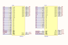
Re: UMBs.. I wouldn't even know where to start on the CPLD.. I've barely even looked at FPGAs (and i have several here that I could mess with).. CPLDs are even further out of my wheelhouse. As for if the lines are going to the 2nd sram chip... based on https://www.vogons.org/download/file.php?id=178492&mode=view and the schematic... there'd be some rewiring to do.. :-( (see attached)
Any ideas on that socket next to U29? Count says theres 40 pins and it's not on the original schematic/board layout.
Attachments
sergey
Veteran Member
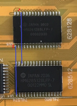
Yeah, pins 1 and pin 30 of U15 (the 128 KiB SRAM) are wired to VCC. Thankfully, it looks that it should be pretty easy to cut these. And next, solder a couple of "blue" wires from corresponding pins of U14... that's the easy part.Re: UMBs.. I wouldn't even know where to start on the CPLD.. I've barely even looked at FPGAs (and i have several here that I could mess with).. CPLDs are even further out of my wheelhouse. As for if the lines are going to the 2nd sram chip... based on https://www.vogons.org/download/file.php?id=178492&mode=view and the schematic... there'd be some rewiring to do.. :-( (see attached)
Any ideas on that socket next to U29? Count says theres 40 pins and it's not on the original schematic/board layout.
CPLD is the difficult part. Ideally, the system designer would be willing to provide the CPLD source code (be that VHDL, Verilog, CUPL or whatever), and then it won't be that difficult to modify it.
Otherwise there are a few ways:
1. Reverse engineer the CPLD code. This is not exactly a rocket science, since the functions of the CPLD are known (pretty much).
2. Build a separate chip select circuit for U15. It would take the A15-A19 address lines (assuming we want 32 KiB granularity) and output the /CS signal to SRAM when 512KiB-640KiB and whatever UMB addresses are accessed.
As a prototype, it is possible to use the SPLD code from my Micro 8088 project, /RAMCS2 equation particularly, but since there are more pins available, it is possible to add more switches to set the UMB addresses

Attachments
where did you get bios 1.0.4? I have 1.0.3...I don't. The first text I see on the screen is your bios. There is a delay before I see your bios screen though. As shown here....
Also, I think I even asked about before.. Still wonder if we can swap out that 128k ram for next one so we can have some UMBs (like the NuXT).. Guess I should look at the schematic again. (btw, I hate newer schematics, I like the old school style where you can follow traces, not just lines with labels.. maybe it's just me)
and... so far my response from the DZT is: "Hello, how much is your mailbox?" Guessing the mean how big of emails I can handle? I dunno.
gmdattilo1
New Member
- Joined
- Nov 15, 2023
- Messages
- 4
I agree, it shouldn't be too different. I was interested in trying to get a VGA signal out to an external monitor without destroying things too much and the schematics might help with that. I was hoping the unpopulated video output header from v1 would still be there. Based on the photo, it looks like its not.I'd think there is not much difference between v2 and v1, other than the CGA circuit was removed and replaced with a header with relevant ISA signals and video output signals.
But it would be nice to get the "official schematic"
Here is the photo of the V2 board on the other forum: https://www.vogons.org/download/file.php?id=178492&mode=view
BTW, it uses 74HC-series, which is BAD decision. These ICs don't have TTL compatible inputs, particularly, the minimal voltage for logic "1" on these, assuming 5V power supply, is 3.3V, while the minimal output of TTL for logic "high" is 2.4V, and typical is 3.4V (well, at least according to the TI SN74LS04 datasheet).
If your ISA boards use TTL or 3.3V CMOS, they will not work well with Book8088
Regarding the potential logic level issues, I have an RTL8019 ethernet card running in the ISA expander. Its ASIC must be compliant with the HC series logic. If anyone is having trouble with ethernet cards, I can vouch that the 8019 works in my unit. Ethernet has been really handy to move files back and forth to a windows computer running an FTP service. I'm using mTCP.
Like sorphin I also do not see the VGA bios message on boot. The screen stays blank for a pretty good while after I power on the system. I am running your v20 v1.0.0 bios, a prepared chip I ordered directly from you. I say that to point out that there is no way the main bios could be suppressing that message, or at least no way that you wouldn't already know about.
Last edited:
From n0p's github. I compiled it and added in my own XTIDE versions.where did you get bios 1.0.4? I have 1.0.3...
@sergey Good news and bad news.. Good news, i heard back, and received files. One of the files is updated "BOOK8088EN20230927最新.docx"... The bad news.. everything else (including the schematic is for the v1).. I poked back at them noting that and requesting the v2 schematic and if they can direct me to the maker if they themselves are not (since it's "DZT's Store" and I've seen DZT in reference to this thing)..
With regard to what you showed above.. that's doable from a hw perspective.. but the CPLD changes... yeah.. more complicated.. See mention above (again) about the 40 pin connector.. Thoughts? maybe a weird debug connector? (bit small for IDE and all the pins are coming directly from the big chip)
gmdattilo1
New Member
- Joined
- Nov 15, 2023
- Messages
- 4
Mine came from "hardcore expert store" but it sounds like your seller provided you with same drawing package that I got. It also included some hand386 stuff.From n0p's github. I compiled it and added in my own XTIDE versions.
@sergey Good news and bad news.. Good news, i heard back, and received files. One of the files is updated "BOOK8088EN20230927最新.docx"... The bad news.. everything else (including the schematic is for the v1).. I poked back at them noting that and requesting the v2 schematic and if they can direct me to the maker if they themselves are not (since it's "DZT's Store" and I've seen DZT in reference to this thing)..
With regard to what you showed above.. that's doable from a hw perspective.. but the CPLD changes... yeah.. more complicated.. See mention above (again) about the 40 pin connector.. Thoughts? maybe a weird debug connector? (bit small for IDE and all the pins are coming directly from the big chip)
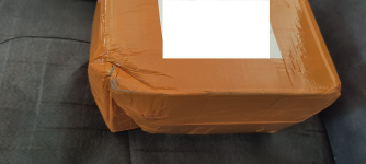
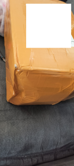
yeah, like I said, the exception is there is the new v2 users guide (which is nice, since my paper one didn't seem as happy either from the packaging fail... (for giggles.. here's how my package looked when it arrived... Amazingly everything was intact though ONLY because of the foam...Mine came from "hardcore expert store" but it sounds like your seller provided you with same drawing package that I got. It also included some hand386 stuff.
Attachments


gmdattilo1
New Member
- Joined
- Nov 15, 2023
- Messages
- 4
did the files your seller sent include one called H-PS2-VGA.pdf? I cant figure out what it is. I also got the v2 guide but like you the same v1 schematics.yeah, like I said, the exception is there is the new v2 users guide (which is nice, since my paper one didn't seem as happy either from the packaging fail... (for giggles.. here's how my package looked when it arrived... Amazingly everything was intact though ONLY because of the foam...
that box looks pretty rough, mine had a much easier ride.
Nope. No such file.did the files your seller sent include one called H-PS2-VGA.pdf? I cant figure out what it is. I also got the v2 guide but like you the same v1 schematics.
that box looks pretty rough, mine had a much easier ride.
sergey
Veteran Member
Oh, forgot to reply to that...Any ideas on that socket next to U29? Count says theres 40 pins and it's not on the original schematic/board layout.
That's a good question, and if we'll get V2 schematic, I bet we'll have an answer. The big chip is the CPLD, and I'd think this is an extension header. Perhaps a trimmed version of ISA bus to connect yet another extension board?
n0p
Experienced Member
Oh, forgot to reply to that...
That's a good question, and if we'll get V2 schematic, I bet we'll have an answer. The big chip is the CPLD, and I'd think this is an extension header. Perhaps a trimmed version of ISA bus to connect yet another extension board?
That's for COM/LPT ports i think, since it looks like they bolted to the case in V2