• Please review our updated Terms and Rules here

Build your own PDP 8I, Part 3..

Hi All;

Dave, Thank You for the confirmation of my Schematic..

"" I can't see anything immediately wrong with either the original schematic or your modified one (other than the original one didn't include DCA or JMS - but that's why we modified it). ""

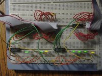
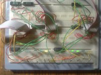
Here is what my Schematic is showing with '0000 and next '7000 loaded..

002.jpg 003.jpg

Some explanation, the first picture is LDIR with '0000 Loaded, the second Picture is with '7000 Loaded..
Also, the Leds from left to right are
B9 pin 6 (JMP.L, JMS.L, DCA.L output)
C1 pins 1 and 2 and 3 ( pin 3 is the Yellow Led)
(Farthest right)
C2 pins 1 and 2 and 13 and 12 (pin 12 is the Yellow Led)..

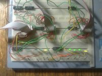
On the BreadBoard, I am going to put the origional in place, Plus the DCA and the JMS, and see if for some reason it behaves differently..

No, Same OutPut..
Pictures to follow..

006.jpg 007.jpg

Dave, Lets go with Your Origional Schematic for Debugging, Except that we will be Substituting the 7410 for the Second 7404.. Since that is What I now have wired up, and it would be what You are most familiar with..

THANK YOU Marty
 
Last edited:
Hi All;

Dave, I have started to do the Debug, and some preliminary Tests..

The 74LS10 pin 6 gows High, when I enter any of these commands..
3000, 4000, 5000..
So this is working correctly..

IR3 on K16 pin 5 is Low when the IR3 Switch is off.. And it is High when the Switch is On.. (1)..

K16 pin 6 is High when the IR3 Switch is off.. And it is Low when the Switch is On.. (1)..

M11 pin 4 is High when the IR3 Switch is off.. And it is Low when the Switch is On.. (1)..

M11 pin 5 is Low when '0000 is entered, and is High when 3000, 4000, 5000 is entered..

M11 pin 6 is High when '0000 is entered, and it is '0000 when 0400 is entered..

M11 pin 6 is Low when 3000, 4000, 5000 is entered..

M11 pin 6 is High when 3400, 4400, 5400 is entered..

G10 pin 1 is High when '0000 is entered, and it is '0000 when 0400 is entered..

G10 pin 1 is Low when 3000, 4000, 5000 is entered..

G10 pin 1 is High when 3400, 4400, 5400 is entered..

G10 pin 2 (IOT) is High no matter what is entered..

G10 pin 13 (Bar MIC) is Low no matter what is entered..

G10 pin 12 is High no matter what is entered..

K15 pin 1 is High no matter what is entered..

K15 pin 2 is Low no matter what is entered..

Now when I am saying " no matter what is entered " I am only refering to the current commands we are testing..
( '0000, '0400, '3000, '3400, '4000, '4400, '5000, '5400)


THANK YOU Marty
 
Last edited:
Let's break this problem down into bits.

G10 pin 2 should be wired back to L5 pin 7. L5 pin 7 should go '0' when 6000 is loaded into IR (we should have already proven this). Therefore G10 pin 2 should also go '0' when 6000 is loaded into IR.

I have wired G10 pin 13 back to L5 pin 9. L5 pin 9 should go '0' when 7000 is loaded into IR (we should have already proven this). Therefore G10 pin 13 should also go '0' when 7000 is loaded into IR.

I will think about the rest tomorrow.

There's your problem at G10 pin 13. A permanent '0' here will mess us up!

In the original it was shown as OPG1 + OPG2. I couldn't find this logical signal - so I just used /MIC.

However, we should sort out the problem with /IOT on G10 pin 2 as well (because this will mess us up later on).

Dave
 
Hi All;

Dave, Thanks for giving me some more Tests and Answers..

"" G10 pin 2 should be wired back to L5 pin 7. L5 pin 7 should go '0' when 6000 is loaded into IR (we should have already proven this). Therefore G10 pin 2 should also go '0' when 6000 is loaded into IR.
YES..

I have wired G10 pin 13 back to L5 pin 9. L5 pin 9 should go '0' when 7000 is loaded into IR (we should have already proven this). Therefore G10 pin 13 should also go '0' when 7000 is loaded into IR.
NO !! As, I have this wired to an inverter after L5 pin 9..

I need to check If it need to be Inverted .. I will looked at my origional Schematic..
I mis-intrepreted the /MIC signal.. I will Correct it, Now..
I am going to Check All of my /MIC and MIC connections..
It is Fixed, and All of them checked for correctness, I think one other one was wrong, because it was connected to G10 pin 13..

"" However, we should sort out the problem with /IOT on G10 pin 2 as well (because this will mess us up later on). ""
OK !!

THANK YOU Marty
 
Last edited:
Hi All;

Here is a ReTest of Dave's Test..

"" IR value => J7 pin 4 value.

0000 => '1' (AND DIRECT)
YES..
0400 => '1' (AND INDIRECT)
YES..
1000 => '1' (TAD DIRECT)
YES..
1400 => '1' (TAD INDIRECT)
YES..
2000 => '1' (ISZ DIRECT)
YES..
2400 => '1' (ISZ INDIRECT)
YES..
3000 => '0' (DCA DIRECT)
YES..
3400 => '1' (DCA INDIRECT)
YES..
4000 => '0' (JMS DIRECT)
YES..
4400 => '1' (JMS INDIRECT)
YES..
5000 => '0' (JMP DIRECT)
YES..
5400 => '1' (JMP INDIRECT)
YES..
6000 => '0' (IOT)
YES
6400 => '0' (IOT)
YES..
7000 => '0' (OPR)
YES..
7400 => '0' (OPR) ""
YES..

Much Better, Now..
Ever so slowly the Bugs are crawling out of their Hiding Places to the surface..

THANK YOU Marty
 
Last edited:
"Ever so slowly the Bugs are crawling out of their Hiding Places to the surface.." - And then Marty bashes them with a big hammer!

Right - so far so good. Let's execute an instruction!!!

Don't get too excited though - it is just a NOP instruction - but this will start to test out the basic instruction fetch and execute logic (and we will start to build on this for the instructions that actually do something later).

First off - we haven't proven that the memory or effective address (EA) logic works properly so we need to prevent this from mucking us around. To this end I propose to prevent the instruction FETCH logic from actually writing an instruction into the Instruction register (IR). We will force an instruction into the IR ourselves and see if it performs correctly. If you haven't already - disconnect the F1 signal from the E11 gate on schematic LD14 with an output pin of 11 (and connect the now disconnected input pin to '1' to prevent it from floating).

We now need to do our STOP and CLEAR buttons as usual.

Use LDPC to store 0000 into the PC.
Use LDIR to store 7000 into the IR.

I will now explain what should happen when you press CONT. The explanation will take much longer than your observation (although you may want to use a slow clock to see what happens - or a variable clock).

When you push CONT, the RUN flip-flop (L9 pin 9) should change state from '0' to '1' and stay at a '1'.

The FETCH flip-flop (L8 pin 9) should change state from a '0' to a '1'. The J6/J5 outputs should then go through the cycle F0, F1, F2, F3 and A4.

On the clock after A4, the FETCH flip-flop (L8 pin 9) should change state from a '1' to a '0'; and the EXEC flip-flop (L9 pin 6) should change state from a '0' to a '1'. The clock pulses should then be generated as before CP0..CP7.

On the clock after CP7, the EXECUTE flip-flop (L9 pin 6) should change state from a '1' to a '0' and the FETCH flip-flop (L8 pin 9) should once again change state from a '0' to a '1'. The cycle should keep repeating FETCH, EXEC, FETCH, EXEC,...

When F0 goes low the PC should be loaded into MA.
When F2 goes low the PC should be incremented.

The PC should, therefore, increment from 0000 on each F2 pulse. When it gets to 7777 (a while...) it should wrap-around to 0000.

Pressing STOP should halt the cycle of events. The RUN flip-flop (L9 pin 9) should go from a '1' to a '0'. The EXECUTE flip-flop should complete its current cycle - but the FETCH flip-flop should not start it's cycle.

Pressing CONT should continue with the next FETCH cycle and repeat as above.

As you have now guessed, you can now store different values in IR for the group 1 microcoded instructions 7XXX and they should perform as expected. For example, 7040 should complement the ACCUMULATOR. Store a meaningful value into the accumulator before you start and watch it 1's complement (hopefully) at each EXECUTE cycle. Ditto with CML (7020) or combined (7060).

Store a value in AC and try and clear it with CLA (7200) or increment it with IAC (7001).

Try the various ROTATE instructions (but don't forget to initialise the LINK register with CLL (7100) or CLL+CML (7120) for one execution (to CLEAR or SET the LINK register) before you start.

You should also be able to try multiple combinations of the set bits for various effects on the ACCUMULATOR and LINK registers. They all should behave as expected. Don't try the group 2 microcoded instructions just yet though.

Dave
 
Hi All;

Dave, Thank You for this very exciting Next step..

"" And then Marty bashes them with a big hammer! ""
I can guarantee that No hammer was used in Debugging is piece of Haedware, even though the Temptation might have been there to do so..

I will do them tomorrow,
On a side note, before when trying to execute a simple instruction, that used the Accumulator, Remember, that It would Clear the Accumulator, like when I did a RAR or an RAL instruction..
I Don't know if we have already fixed that or Not.. Tomorrow will tell..
But, that means that maybe it should be something for You to think about..
Even, though I have not proved that this is still true..

THANK YOU Marty
 
Last edited:
"On a side note, before when trying to execute a simple instruction, that used the Accumulator, Remember, that It would Clear the Accumulator, like when I did a RAR or an RAL instruction..
I Don't know if we have already fixed that or Not.. Tomorrow will tell.."

Well, a few things have been fixed up to now. This is the next logical step - so let's see what happens! (But I will have a think about it in the meantime).

Dave
 
Hi All;

Dave, Thank You for the Tests..

"" Don't get too excited though - it is just a NOP instruction - but this will start to test out the basic instruction fetch and execute logic (and we will start to build on this for the instructions that actually do something later).

First off - we haven't proven that the memory or effective address (EA) logic works properly so we need to prevent this from mucking us around. To this end I propose to prevent the instruction FETCH logic from actually writing an instruction into the Instruction register (IR). We will force an instruction into the IR ourselves and see if it performs correctly. If you haven't already - disconnect the F1 signal from the E11 gate on schematic LD14 with an output pin of 11 (and connect the now disconnected input pin to '1' to prevent it from floating).
Already Done..
We now need to do our STOP and CLEAR buttons as usual.

Use LDPC to store 0000 into the PC.
Use LDIR to store 7000 into the IR.
OK..
I will now explain what should happen when you press CONT. The explanation will take much longer than your observation (although you may want to use a slow clock to see what happens - or a variable clock).

When you push CONT, the RUN flip-flop (L9 pin 9) should change state from '0' to '1' and stay at a '1'.
YES..
The FETCH flip-flop (L8 pin 9) should change state from a '0' to a '1'. The J6/J5 outputs should then go through the cycle F0, F1, F2, F3 and A4.
YES..
On the clock after A4, the FETCH flip-flop (L8 pin 9) should change state from a '1' to a '0'; and the EXEC flip-flop (L9 pin 6) should change state from a '0' to a '1'. The clock pulses should then be generated as before CP0..CP7.
YES..
On the clock after CP7, the EXECUTE flip-flop (L9 pin 6) should change state from a '1' to a '0' and the FETCH flip-flop (L8 pin 9) should once again change state from a '0' to a '1'. The cycle should keep repeating FETCH, EXEC, FETCH, EXEC,...
YES..
When F0 goes low the PC should be loaded into MA.
When F2 goes low the PC should be incremented.
YES..
The PC should, therefore, increment from 0000 on each F2 pulse. When it gets to 7777 (a while...) it should wrap-around to 0000.
I have done this before, But, since we made some changes, I will let it do it again..
YES..
Pressing STOP should halt the cycle of events. The RUN flip-flop (L9 pin 9) should go from a '1' to a '0'. The EXECUTE flip-flop should complete its current cycle - but the FETCH flip-flop should not start it's cycle.
YES..
Pressing CONT should continue with the next FETCH cycle and repeat as above.
YES..
As you have now guessed, you can now store different values in IR for the group 1 microcoded instructions 7XXX and they should perform as expected. For example, 7040 should complement the ACCUMULATOR. Store a meaningful value into the accumulator before you start and watch it 1's complement (hopefully) at each EXECUTE cycle. Ditto with CML (7020) or combined (7060).

Store a value in AC and try and clear it with CLA (7200) or increment it with IAC (7001).

Try the various ROTATE instructions (but don't forget to initialise the LINK register with CLL (7100) or CLL+CML (7120) for one execution (to CLEAR or SET the LINK register) before you start.

You should also be able to try multiple combinations of the set bits for various effects on the ACCUMULATOR and LINK registers. They all should behave as expected. Don't try the group 2 microcoded instructions just yet though. ""

"" For example, 7040 should complement the ACCUMULATOR. ""
YES !!!!!
"" Ditto with CML (7020) ""
YES..
"" Ditto with CML (7020) or combined (7060). ""
YES..
"" Store a value in AC and try and clear it with CLA (7200) ""
YES..
"" increment it with IAC (7001).
YES !!!!
"" (but don't forget to initialise the LINK register with CLL (7100) or CLL+CML (7120) for one execution (to CLEAR or SET the LINK register) ""
YES, and I was able to put a Value in the ACC and it did NOT clear it.. And I Could complement the ACC and the Link Register still Set, and I could Clear the Link Bit, and the ACC was left alone..
I have complemented the Link Bit (7020) and Done a Rotate RAR (7010) and it Rotates all the way thru the Accumulator and Back to the Link Bit..
I have complemented the Link Bit (7020) and Done a Rotate RAL (7004) and it Rotates all the way thru the Accumulator and Back to the Link Bit..
I Set a Bit in the Accumulator and did a Rotate RAR (7010) and it Rotates all the way thru the Accumulator and Back to the Link Bit..
I Set a Bit in the Accumulator and did a Rotate RAL (7004) and it Rotates all the way thru the Accumulator and Back to the Link Bit..
And It didn't Erase the Accumulator before hand..
I need to go Look at the group 1 Instructions, to see what they are and to make sure I have done them all..
The only Instruction I hadn't tried was Double Rotate (0002) added to a Rotate instruction and it Works, both directions !!

THANK YOU Marty
 
Last edited:
Looking good there Marty...

The CLA/CLL occurs first (if the bit(s) is/are set) and should occur in CP0.

The CMA/CML occurs second (if the bit(s) is/are set) and should occur in CP2.

The IAC occurs third (if the bit is set) and should occur in CP3.

RAR/RTR/RAL/RTL then occur last in this order during CP4,5,6 and 7.

So, if the CLA bit is set - the ACCUMULATOR will always be cleared during CP0. To test this, load any value into AC (using LDAC) and then 'CONT' the PDP-8 machine with your desired instruction. AC should be cleared as expected.

If the CLA bit is not set, then whatever is in the ACCUMULATOR at the beginning of the instruction will be modified by the instruction. As the instruction 'loops' this will cause the value in the ACCUMULATOR to be modified in a known pattern. So for example, CLA + IAC (7201) should guarantee that AC is cleared first in CP0 and then INCREMENTED in CP3 - so the value in AC will be 0001 after execution of the instruction (irrespective of what was in AC prior to the CONT button being pressed). Processing IAC (7001) on its own, however, will cause the value in the accumulator to be incremented once on each execution of the instruction - so the AC value could start off at 0000 and increment to 777 and then wrap around to 0000.

Combining some of the instruction bit patterns will result in specific values in the ACCUMULATOR (taken from http://homepage.cs.uiowa.edu/~jones/pdp8/man/mri.html and http://homepage.cs.uiowa.edu/~jones/pdp8/man/micro.html):

CLA (0)
CLA IAC (1)
CLA CLL CML RTL (2)
CLA CLL CML RTR (1024)
CLA CMA CLL RAR (2047)
CLA CLL CML RAR (2048)
CLA CMA (4095)
CLA CMA CLL RAL (4094)
CLA CMA CLL RTL (4093)

The number in the () is the (decimal) number that should be stored in the ACCUMULATOR at the completion of the instruction. To determine the instruction bit pattern, logically 'OR' the octal number for each of the separate instructions together:

CLA IAC = 7200 'OR' 7001 = 7201.

You will also find some 'wierd' instruction patterns. For example, CLA CMA IAC = 7200 'OR' 7040 'OR' 7001 = 7241. This instruction should clear the ACCUMULATOR in CP0, Then complement the ACCUMULATOR in CP2 and then increment the ACCUMULATOR in CP3. Net result, the accumulator should be cleared at the conclusion of the instruction irrespective of the value in the ACCUMULATOR at the start...

I would suggest becoming familiar with the OPR Group 1 instructions and how they operate, trying to identify what should occur, testing them out on the PDP-8 and seeing if they fit with your understanding. If not, report back what you are trying to achieve and the conflicting results you are getting and I will try and dispel the mists so to speak.

I am working on the OPR Group 2 tests now - but these are a bit more complex than the Group 1 tests...

Dave
 
Last edited:
Hi All;

Dave, Thanks for the next set of Tests and the Test from the Posting after this Post and for the Complement..

I have to get a few things done around here, I am not sure How long it will take, So it will be after I get things done..
I Think I am Done, I will know tonight.. The last few days the Heater has been running excessively and so today, I hopefully sealed the Cold Air leak(s) here in the kitchen..

"" Looking good there Marty...

The CLA/CLL occurs first (if the bit(s) is/are set) and should occur in CP0.

The CMA/CML occurs second (if the bit(s) is/are set) and should occur in CP2.

The IAC occurs third (if the bit is set) and should occur in CP3.

RAR/RTR/RAL/RTL then occur last in this order during CP4,5,6 and 7.

So, if the CLA bit is set - the ACCUMULATOR will always be cleared during CP0. To test this, load any value into AC (using LDAC) and then 'CONT' the PDP-8 machine with your desired instruction. AC should be cleared as expected.

If the CLA bit is not set, then whatever is in the ACCUMULATOR at the beginning of the instruction will be modified by the instruction.
YES..
As the instruction 'loops' this will cause the value in the ACCUMULATOR to be modified in a known pattern. So for example, CLA + IAC (7201) should guarantee that AC is cleared first in CP0 and then INCREMENTED in CP3 - so the value in AC will be 0001 after execution of the instruction (irrespective of what was in AC prior to the CONT button being pressed).
YES..
Processing IAC (7001) on its own, however, will cause the value in the accumulator to be incremented once on each execution of the instruction - so the AC value could start off at 0000 and increment to 777 and then wrap around to 0000.
YES..
Combining some of the instruction bit patterns will result in specific values in the ACCUMULATOR (taken from http://homepage.cs.uiowa.edu/~jones/pdp8/man/mri.html and
http://homepage.cs.uiowa.edu/~jones/pdp8/man/micro.html ..
CLA (0)
YES..
CLA IAC (1)
YES..
CLA CLL CML RTL (2) CLA, 7200 : CLL, 7100 : CML , 7020 : RTL, 7006..
This Works !!
CLA CLL CML RTR (1024) CLA, 7200 : CLL, 7100 : CML , 7020 : RTR, 7012..
I Think This Works..
CLA CMA CLL RAR (2047) CLA, 7200 : CLL, 7100 : CML , 7020 : RAR, 7010..
This shows Bit '0'..
CLA CLL CML RAR (2048) CLA, 7200 : CLL, 7100 : CML , 7020 : RAR, 7010..
This Works !!
CLA CMA (4095) CLA, 7200 : CMA, 7040..
All Ones, except the Link Bit..
CLA CMA CLL RAL (4094) CLA, 7200 : CMA, 7040 : CLL, 7100 : RAL, 7004..
The Link Bit and all of the Bits, Except for bit 11..
CLA CMA CLL RTL (4093) CLA, 7200 : CMA, 7040 : CLL, 7100 : RTL, 7006..
The Link Bit and all of the Bits, Except for bit 10..

The number in the () is the (decimal) number that should be stored in the ACCUMULATOR at the completion of the instruction. To determine the instruction bit pattern, logically 'OR' the octal number for each of the separate instructions together:

CLA IAC = 7200 'OR' 7001 = 7201.
YES..
You will also find some 'wierd' instruction patterns. For example, CLA CMA IAC = 7200 'OR' 7040 'OR' 7001 = 7241. This instruction should clear the ACCUMULATOR in CP0, Then complement the ACCUMULATOR in CP2 and then increment the ACCUMULATOR in CP3. Net result, the accumulator should be cleared at the conclusion of the instruction irrespective of the value in the ACCUMULATOR at the start...

NO, But, Each Instruction works individually, But, not together..
I have ohmed out each Individual Instruction, and they are each at the Correct CPxx time..
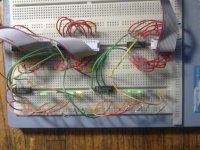
I suspect a Bad or marginally Bad IC, I am going to put it on the BreadBoard, with Lots of Leds, to see who is not getting thru correctly..
Dave, I know 'What' I should get, it's Just not happening.. I think I can find it.. I will let You Know what I find..
I see the Problem, there isn't enough time, between CP02 and CP03 for the gate to switch back after the pulse,
I am going to try and Delay Cp03 and see if that makes any difference..
No, it doesn't, I will have to bring out the other IC tomorrow morning, to see if the other IC something is holding the signal for too Long..
Dave, I have E12 and G1 on one IC, and G15 is the one I already brought out.. These are on the AC(L) schematic..
Lots of stringly wires on the BreadBoard and more Leds..

I would suggest becoming familiar with the OPR Group 1 instructions and how they operate, trying to identify what should occur, testing them out on the PDP-8 and seeing if they fit with your understanding. If not, report back what you are trying to achieve and the conflicting results you are getting and I will try and dispel the mists so to speak.

I am working on the OPR Group 2 tests now - but these are a bit more complex than the Group 1 tests... ""
GREAT !!!!!!!!!
Go ahead and Post them, when You have them ready, Even if I haven't gotten to these Tests, More Input..
I don't know, But, I suspect that these Group 2 Tests, will be the next big trouble, But, then again it could be Memory related..
Since it passed the RAR and RAL at least through the Instruction Register..


"" The non-skip part of the Group 2 instructions... I will work on the SKIP part of the Group 2 instructions and post later when I get a bit of time myself.

STOP and CLEAR buttons (this should be automatic now on power-up!)

Load 7402 into IR manually.
Load 1234 into AC manually.
Load 0000 into PC manually.

CONT.

The PDP-8 should halt with the PC advanced from 0000 to 0001. The AC should still have 1234 in it. This is the intended action because a 7402 instruction is HLT...
YES..
CONT.

The PDP-8 should halt once again with the PC advanced from 0001 to 0002. The AC should still have 1234 in it.
YES..
Try a few more CONTs. The PC should increment by 1 every time but the AC should retain 1234.
The MA Register follows the PC Register..
Load 7612 into IR manually.

CONT.

The PDP-8 should halt again (with the PC incremented by 1 again from the value before CONT was pressed) but the AC should have been cleared to 0000. 7612 = CLA HLT.
YES..
Load 7614 into IR manually.

CONT.

The PDP-8 should run continuously this time (there is no HLT bit set). 7614 = CLA OSR.

The value entered onto the handkeys should appear in the ACCUMULATOR. The PC should increment by 1 for each instruction executed.
YES, I checked each Bit Individually..
STOP.

Clear the hand keys to 0000.

Load 0000 into AC manually.
Load 7404 into IR manually.

CONT.

The PDP-8 should run continuously this time (there is no HLT bit set). 7404 = OSR.

When a handkey is set to '1' the corresponding bit should be set in the ACCUMULATOR. When the hand key is set to '0' the corresponding bit in the ACCUMULATOR should remain a '1'. This instruction OR's the hand keys with the ACCUMULATOR and stores the result in the ACCUMULATOR. ""
YES..

THANK YOU Marty
 
Last edited:
That's one of the reasons why I have gone down the route I have in ignoring the memory. We can test the OPR instruction in isolation from the others and then move on to the memory next. This way we rule out most (but not all) of the MUX/ALU and register wiring from the equation.

The non-skip part of the Group 2 instructions... I will work on the SKIP part of the Group 2 instructions and post later when I get a bit of time myself.

STOP and CLEAR buttons (this should be automatic now on power-up!)

Load 7402 into IR manually.
Load 1234 into AC manually.
Load 0000 into PC manually.

CONT.

The PDP-8 should halt with the PC advanced from 0000 to 0001. The AC should still have 1234 in it. This is the intended action because a 7402 instruction is HLT...

CONT.

The PDP-8 should halt once again with the PC advanced from 0001 to 0002. The AC should still have 1234 in it.

Try a few more CONTs. The PC should increment by 1 every time but the AC should retain 1234.

Load 7612 into IR manually.

CONT.

The PDP-8 should halt again (with the PC incremented by 1 again from the value before CONT was pressed) but the AC should have been cleared to 0000. 7612 = CLA HLT.

Load 7614 into IR manually.

CONT.

The PDP-8 should run continuously this time (there is no HLT bit set). 7614 = CLA OSR.

The value entered onto the handkeys should appear in the ACCUMULATOR. The PC should increment by 1 for each instruction executed.

STOP.

Clear the hand keys to 0000.

Load 0000 into AC manually.
Load 7404 into IR manually.

CONT.

The PDP-8 should run continuously this time (there is no HLT bit set). 7404 = OSR.

When a handkey is set to '1' the corresponding bit should be set in the ACCUMULATOR. When the hand key is set to '0' the corresponding bit in the ACCUMULATOR should remain a '1'. This instruction OR's the hand keys with the ACCUMULATOR and stores the result in the ACCUMULATOR.

Dave
 
"NO, But, Each Instruction works individually, But, not together..".

I didn't bring my schematic diagrams in to work with me today - and I have something on this evening - but hopefully I will find a little bit of time to have a look and suggest something for you to have a look at.

I think now we are getting to the heart of problem that has been there all along.

I have come up with a set of tests for the OPR Group 2 skips - but we need to squash this bug first I think.

Dave
 
Hi All;

Dave, Thank You for Your insight..

"" I think now we are getting to the heart of problem that has been there all along.
You may be right, I am setting up the BreadBoard, having a look see at what is happening..

I have come up with a set of tests for the OPR Group 2 skips - but we need to squash this bug first I think. ""
OK..

THANK YOU Marty
 
Marty,

I don't think the problem is with the AC(L) logic on schematic LD15 - but with where the clocks are derived from.

The AC(L) signal is a LEVEL (unlike all the other XX(L) signals which are pulses - clocks - themselves).

Where does the clock come from for L10 pin 2 (Schematic LD9 SN74163 clock pin)?

Where does the clock come from for F9,10 and 11 pin 11 on schematic LD19 (the accumulator itself).

If the clocks originate from the same source - then you have a potential race hazard - and whatever gets loaded into AC will depend on the 'butterfly in the tropics' (aka crosstalk amongst all those wires on your board).

I wil have a look at my own schematic later. I am running out of the door now for a prior engagement. EDIT: Just answered my own question - they both come from CLOCK_H so I suspect a race hazard. I will see what we can do about that later. This is a limitation of simulation - it doesn't fully simulate reality!

Dave
 
Hi All;

Dave, Thank You for YourInsight,

"" I don't think the problem is with the AC(L) logic on schematic LD15 - but with where the clocks are derived from.

The AC(L) signal is a LEVEL (unlike all the other XX(L) signals which are pulses - clocks - themselves).

Where does the clock come from for L10 pin 2 (Schematic LD9 SN74163 clock pin)?
Master CLK.H
Where does the clock come from for F9,10 and 11 pin 11 on schematic LD19 (the accumulator itself).
Master CLK.H
If the clocks originate from the same source
YES..
- then you have a potential race hazard - and whatever gets loaded into AC will depend on the 'butterfly in the tropics' (aka crosstalk amongst all those wires on your board). ""

Dave, I earlier modified Your Clock circuit, and I Liked it's outPut a little better, Then I went back to Your Circuit and tried another thing..
I put on the BreadBoard a 74LS138, and wired it up so it would work like the 74LS42..
I then tied the G1 Enable signal to the clock pulse, pin 5..
And by doing this I have two distinct pulses coming out of AC(L), one for CP02 and one for CP03..
It still does not quite work, so I hope to tweak this a little..
My clock circuit takes pin 2 on the 7474 and instead of having it tied to pin 6, I tie it to pin 8, and the other thing I need to retry is I tied pin 11 to pin 3, this slows the Clock down quite a bit, so I left it tied to pin 11..
I am thinking You are right, as it almost works, but not quite..
Where would the Clock pulse then come from for F9, F10 and F11, I could try tieing it to AC(L) ??
I will look at the Equations for AC(L)..
I tried this as well, No good..
OR taking Clock.L and Delaying it, Ie, putting it thru an odd number of inverters, so it would be Clock.H (delayed)..
In one of the WireLists, it had a Delay of One inverter between the AC(L) and the RAR, RAL, but it didn't work, as it was the Wrong polarity..
I am going to try this only, I will use a 7408 for one gate delay, OR two 7404's for a two gate delay on the BreadBoard..
Why not, I have time to wait till Dave can figure it out, and who knows, maybe this will help..
This didn't Help, I tried one, two and four gate Delay..
But, maybe taking Clock.L and putting thru one inverter, will be enough of a delay to cancel the 'Race' Condition..
I will try this next, This will be more work..
No, I tried with one and three gate Delays, the clock to the 74194's, makes No difference, that I can tell..
At present I can attach 'anything' to the 74194's Clock pin (11), as I have them Isolated, The former wire to them is unwired and Taped off..
Dave, You know more about this than I do..
I hope that this in a small way Helps, But probably it won't, knowing my grasp of the situation..

I re-attached the clock pin (11) of the 74194's back to the Master Clock.H Via a Jumper for the Tests below..
We'll I guess that what I can do next is, try some more of the Tests, and see what results I get..
I Think All of the Other Tests Passed ..
I was Only after running All of the Other Tests, and so Noticing the Link Bit and then doing as described below that I found..

!!!!!!!!!!!!!!!!!!!!!!!!!!!!!!!!!!!!!!!!!!!!!!!!!!!!!!!!!!!!!!!!!!!!!!!!!!!!!!!!!!!!!!!!!!!!!!!!!!!!!!!!!!!!!!!!!!!!!!!!!!!!!!!!!!!!!!!!!!!!!!!!!!!!!!!!!!!!!!!!!!!!!
After Re-Reading the paragraph, My Intrepretation of what was written was WRONG !!!
So there was and IS NO PROBLEM !!!!!!!!!!!!!!!!!!!!!!!!!

"" You will also find some 'wierd' instruction patterns. For example, CLA CMA IAC = 7200 'OR' 7040 'OR' 7001 = 7241. This instruction should clear the ACCUMULATOR in CP0, Then complement the ACCUMULATOR in CP2 and then increment the ACCUMULATOR in CP3. Net result, the accumulator should be cleared at the conclusion of the instruction irrespective of the value in the ACCUMULATOR at the start... ""

This Sets the Link Bit, NOT Bit 11 !!!!!
I was looking for Bit 11 to be set after the Accumulator was Complemented and a 1 was added..

I had not, never noticed that the Link Bit was being Set, while trying to Run this group of Instructions..

"" I have come up with a set of tests for the OPR Group 2 skips ""
So, Now You can Bring them on..

I can Now Wire Back the 74194's to the Clock.. Done..

Because of My Mistake and wasting a day, I am going to do what I hadn't thought of to do Before..
I am going to Move (put in another Led and Dis-attach the old one, but leave it in place) the Led for the Link Bit and put it Next to the Accumulator where it belongs..
I am also going to do the same kind of thing for the various LoaDxx Leds only they will be offset slightly..
Where they can do some good..

THANK YOU Marty
 
Last edited:
I had a quick look at the problem this morning and think I have found a solution - I haven't tested it though as I have gone down with a 'bug' (not the software or hardware kind though) so I am not thinking 100% straight...

The problem is that the main 'system' clock (for the state machine CPx etc.) is the same clock that is being used to latch the data into the registers. This is a poor design. The problem we originally had was setting and clearing the MA(L) signals etc at virtually the same time. To overcome this I came up with my little clock circuit to delay the clearing of the MA(L) flip-flop by half a clock cycle. However, this leaves the problem (as you have found out) that the CPx signals are changing at exactly the same time as the clock signal to latch the new data into the registers - leading to a race.

I think the 'fix' is relatively simple (but this maybe my fever talking of course).

In my clock circuit I had a CLOCK_H (which goes to all the logic) and a CLOCK_L that was used to reset the MA(L) flip-flop (and the others).

What my proposal is is to leave CLOCK_H for the bulk of the logic and use the CLOCK_L signal as the clock for the ACCUMULATOR clocking (F9, F10 and F11 pin 11 on schematic LD19), the LINK flag clock (H13 pin 4) and for the clock for the flip-flops for MB(L), MA(L), PC(L) and IR(L). I would then use the inverted CLOCK_H signal to feed the 'CLR' input (via the NAND gate) of the flip-flops for MB(L), MA(L), PC(L) and IR(L). I hope that makes sense.

The basis of operation should be a high-going CLOCK_H signal to step the state machine. A bit of time for signals to stabilise. A high-going CLOCK_L signal to latch things into the registers. A bit of time for the action to complete. A high-going /CLOCK_H signal to reset the flip-flops used for latching the data into MA(L) and its siblings. Note the key thing 'a bit of time to stabilise'...

I notice you mentioning the LINK register. All we have proven so far is that we should be able to SET and COMPLEMENT the link register using CPR Group1 instruction - nothing else!!! You may be right and there is a problem here - but without identifying a specific set of tests we are just 'stabbing in the dark'.

Dave
 
Hi All;

Dave, Thank You for the System Clock analysis..

I am Sorry that You have caught a 'BUG'..

I am not feeling so good myself this morning, but it just might be a early morning thing, hopefully not Your 'Bug'..

I am going to try and make my way thru Your steps, I am a little confused.. But, I figure If I do them a sentence at a time and put down the results, hopefully we can get somewhere..

"" In my clock circuit I had a CLOCK_H (which goes to all the logic) and a CLOCK_L that was used to reset the MA(L) flip-flop (and the others).

What my proposal is is to leave CLOCK_H for the bulk of the logic and use the CLOCK_L signal as the clock for the ACCUMULATOR clocking (F9, F10 and F11 pin 11 on schematic LD19), the LINK flag clock (H13 pin 4) and for the clock for the flip-flops for MB(L), MA(L), PC(L) and IR(L). I would then use the inverted CLOCK_H signal to feed the 'CLR' input (via the NAND gate) of the flip-flops for MB(L), MA(L), PC(L) and IR(L). I hope that makes sense.

The basis of operation should be a high-going CLOCK_H signal to step the state machine. A bit of time for signals to stabilise. A high-going CLOCK_L signal to latch things into the registers. A bit of time for the action to complete. A high-going /CLOCK_H signal to reset the flip-flops used for latching the data into MA(L) and its siblings. Note the key thing 'a bit of time to stabilise'...


THANK YOU for Your Help !!! Get Better Soon !!!


"" What my proposal is is to leave CLOCK_H for the bulk of the logic
OK..
and use the CLOCK_L signal as the clock for the ACCUMULATOR clocking (F9, F10 and F11 pin 11 on schematic LD19),
the LINK flag clock (H13 pin 4) ""
I'LL try this first..
OK, it's temporily wired via IC Clips, and it seems to be working OK..
It's Now wired in that Way..
"" and for the clock for the flip-flops for MB(L), MA(L), PC(L) and IR(L).
OK, After reading this a couple of times, I make this a Clock.L also..
OK. I will try this next
"" I would then use the inverted CLOCK_H signal to feed the 'CLR' input (via the NAND gate) of the flip-flops for MB(L), MA(L), PC(L) and IR(L). I hope that makes sense. ""
I am confused about this..
Do You mean like on (for the IR) G7 pin 4, that I use Clock.H OR do I Invert Clock.H and feed it to G7 pin 4 ???
I will use the BreadBoard on these and see what I can find out..

I put all three IC's on the BreadBoard, and then I just traded the cable signals and the IC signals for the IR(L) only and tried it.. The IR(L) does seem to work OK, that way..
I am also going to try Inverting the Clock.L and then feed that into the Nand gate..
And see If that makes any difference..
No, it doesn't make any difference..
So, I will wire this up, and test all of the xx(L) outputs..
Ok, the Change has been made, and they all do seem to be better, but it could be my imagation..
I have done a simple test a Rotating 1's on all of the registers, and they all are doing fine..
Also, even though we haven't officially tested it yet.. But, the Deposit and the Examine seem to Work, Better/right, they Increment Now, and would not always do so before..

Also, I am not going to be able to wire up the various xx(L) signals next to their Display and the Link Bit as well where I wanted them to be, No Room on the Board, unless I do a major re-wiring and moving of the Led Driver's..
I will move the Link Bit, to a closer place, But it is not exactly where I would Like it.. If I don't like it then I guess I will need to do some moving of the Led Drivers..

THANK YOU Marty
 
Last edited:
Take the CLOCK_H signal and feed it into an inverter. Take the output of the inverter and feed it into G7 pin 4 (for IR(L)).

If you don't want to use an inverter - you can take the signal for G7 pin 4 from the 'opposite' side of the flip-flop that generates CLOCK_H (you get both the normal and inverted sense of a signal from the Q and /Q outputs of a flip-flop respectively for free).

Hope that makes more sense.

Feeling a bit better now thanks - I have spent most of the afternoon asleep with the TV on watching Futurama in between waking up and going back to sleep.

I have just read the rest of your post - a little warning. If you invert CLOCK_L and feed and feed that into the NAND gate at G7 pin 4 we have put the circuit back again so that the clock and clear of the IR(L) latch are effectively generated by the same signal and it is a 'crap shoot' again as to whether this will work.

Dave
 
Hi All;

Dave, Thanks for Your Answer..

What I did was take the signal (CLK.L) from G7 pin 4 and put it to G6 pin 11, and I took the signal (CLK.H) from G6 pin 11 and put it to G7 pin 4..

Also, Remember this has been done for ALL of the XX(L)'s.. IR(L), PC(L) etc..

If this is NOT what You ment, then Please enlighten me, where to get the Inverted Signal without using another Inverter..

"" you can take the signal for G7 pin 4 from the 'opposite' side of the flip-flop that generates CLOCK_H (you get both the normal and inverted sense of a signal from the Q and /Q outputs of a flip-flop respectively for free). ""

Are You refering to the 7474 clock divider for making CLK.H and CLK .L OR to pin 8 of G6.. Remember I copied Your Clock divider from Your Schematic using a 7474..

"" you get both the normal and inverted sense of a signal from the Q and /Q outputs of a flip-flop respectively for free). ""
I Knew this.. But, Thanks for the reminder..

THANK YOU Marty
 
Back
Top