sponaugle
Member
I have a couple of 5170 systems, and one of them has significant number of bad DRAMs. While you can still get some of stacked DRAMs from ebay, the supply isn't huge, and the cost to replace all 512K is pretty high. Based on a conversation between a few other members a while back:
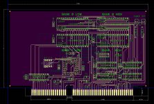
I thought it would be fun to make an ISA 16-bit memory card that could replace all of the system memory, including the onboard DRAM. This will require a small modification to the main board, as well as a 16-bit memory card that can provide the needed memory mappings.
I thought it valuable to start a new thread to encompass the design and build work.
This is a relatively simply ISA card, and I have done some ISA card design back in the 90s as well as a few PCI cards in the 2000s, but it seems most of that has faded from my memory!
The goal is to have a 16bit (only) ISA memory card that has somewhere between 1 and 4 MB of SRAM, and is capable of mapping that SRAM into any part of the system memory. Constraints: SRAM only, no DRAM so no REFRESH. Through hole mount components if possible for easy building. Surface mount version would be doable, but if we can get a though hole first that would be preferred. All components available new from Digikey/Mouser/etc.
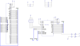
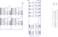
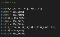
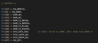
I am going to use DipTrace for the schematic design and PCB design, which is a departure from the usual KiCad or other popular tools - Only because I have used it a lot, and it is a very fast to learn environment. As far as parts selection, I want this first version to be very flexible so I'm going to use an ATF1504 CPLD. It is a PLCC-44 part, so through hole socket support, JTAG programming, 7ns, and very flexible. The design langauge (CUPL) is very easy to write and follow (although the actual tool WinCUPL is a masterpiece of frustration!). For the RAM I'll use the AS6C4008s, a 512kx8 through hole SRAM that you can buy new today, 5V, and 55ns so plenty fast enough.

