• Please review our updated Terms and Rules here

CGA Card With Unknown MOD

charlysan

Member
Joined
Apr 8, 2023
Messages
38
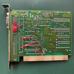
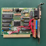
I recently received a Juko XT clone PC that has two CGA cards connected to the board. One of those CGA cards has the following mod:

ICs:

#1 -> PAL16R4ACN
#2 -> DS26LS31CN


cga_mod_front_a.png

cga_mod_back_a.png

For the moment, I have done the following tests:

1. Connect the modded CGA card to another Juko board (A: standalone; B: along with another CGA card; C: along with an Hercules card)

2. Connect a Logic analyzer to DB9 port:

* HSYNC: high
* VSYNC: low
* RGB pins: High

I get no sync or video signal. All pins stay in the state described above.

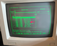
3. Checkit reports 32K Hi RAM:

1694117077055.png


Does anybody recognize this kind of mod?
 
Looks like it was modded to coexist with a standard CGA. If the memory and I/O has been moved, the system BIOS isn't going to initialize the card. Probably needs some special software.
 
I agree. But... why this line driver and all these lines to the D-connector? THAT puzzles me.
Exactly. I will do additional tests in the following days. This PC had a ST-238R HDD + ST 11R controller. Once I can read the data in the hard drive I might be able to find the software used for this thing. And BTW, I might need some help with the ST-238R, as this is the first time I have one of those.
 
Last edited:
I agree. But... why this line driver and all these lines to the D-connector? THAT puzzles me.

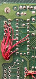
It looks like the guy who did this very neatly obliterated the traces between the D-connector and the output latch. +1 for craftmanship?

Running the differential lines to the D-connector doesn’t leave enough connectors to package all of CGA’s signals; you need at least six plus ground (RGBI+H/Vsync), it looks like they’re only getting four. Can you trace out which four they are? If it’s just the video data lines and sync isn’t making it in somehow then it’s very puzzling what this might be for. Alternatively they may be packing up just the sync signals and, say, G+I, because they were driving a monochrome monitor over a really long tether?
That's correct, some traces have been cut:

IMG_FAD2B0914FBB-1.jpeg

I will trace them out, and upload a schematic soon.

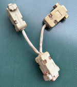
Another thing I haven't mentioned: they were using a DB9-Y cable, so I guess they were driving two monitors in parallel from one of the cards. I have already tested out the splitter with two monochrome monitors and an Hercules card, and it works OK.

1694186249270.png
 
Just eyeballing this it looks to me like they're picking up the red, green, blue, and vsync signals from the broken traces to send to that line driver? I can't be sure about that, the wires are too dense over the lower end of the plug.

Vsync alone wouldn't be enough to drive a monitor; is it possible they're grabbing hsync from somewhere else and combining them with the PAL so the buffer is outputting an RGB+Csync signal?

I'm starting to wonder if this might have been used to drive a large, ancient projector system or something; at the other end of the long differential cable there was a simple resistor setup after the matching receiver that shoveled this straight into a SCART-style RGB. It'd only be 8 colors, not 16, but good enough for whatever they were doing with it?
 
@Eudimorphodon, your assumptions were correct.

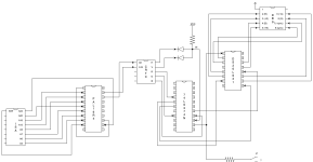
After following the traces using a multimeter, I got these schematics:

1694546063103.png


Some conclusions can be taken from the above diagram:

1 - HSYNC and VSYNC are combined into CSYNC, which then goes to 74LS374 latch.
2 - The card is sending R, G, B and CSYNC through DB connector, using differential lines (R, ~R; G, ~G; B, ~B, CSYNC, ~CSYNC).
3 - PLD is only used to change card default ports and memory addresses

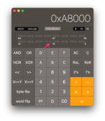
Traces A6 and A16 going through CRTC ASIC and ISA connector have ben cut off, and new connections were made from PLD. And taking into account tat the default CGA buffer addresses is 0xB80000, we should be able to deduce the new address by changing bit A16:
1694540507391.png
And 0xA8000 is what was found by Checkit as Hi RAM, so it makes sense.

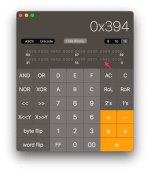
Same thing with CGA ports: 0x3D4, 0x3D5, 0x3D8, 0x3D9:
1694540426315.png

And those will become: 0x9D4, 0x395, 0x398, 0x399 after changing bit A6

That information should be enough to try to initialize the card. For that, I grabbed vcol.asm example from "PC System Programming" (Thanks @modem7 for sharing the PSP floppies), that can be used to write to CGA card without using the BIOS; and then I changed the default addresses:

CONTROL_REG = 0398h ;Control register port address
CCHOICE_REG = 0399h ;Color select register port address
ADDRESS_6845 = 0394h ;6845 address register
DATA_6845 = 0395h ;6845 data register
VIO_SEG = 0A800h ;Video RAM segment address


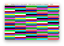
After compiling and linking with MASM, I tried it out first with DOSBOX (I compiled two versions, one using the default address and another one with the new ones):
1694541060626.png
That's the pattern that should be generated by the modded CGA card.

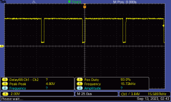
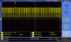
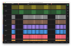
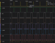
Next step was to run that on a real PC with the modded CGA card inserted. I immediately got some signals out from DB connector:
1694541216231.png
1694542809959.png


And then I captured a single frame (1 HSYNC period) and tried to render it; and I got the expected pattern in 8 colors (no intensity bit):
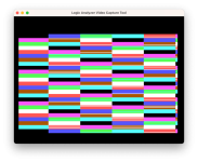
1694541378204.png

There are some errors in the image, probably because I have a bug in my capturing/rendering script.


There is only one thing left to figure out: I don't know the purpose of that line connecting CSYNC to J1 jumper. If somebody has the jumper documentation for this card, it will be very useful to understand what is going on there.
 
Last edited:
Hah! I guess I get a gold star for wild guessing.

The $64,000 question that might forever be left unanswered is what in the world this thing was originally used for. Maybe they built this because they needed to send video over existing twisted pair wiring in a building, and it drove some kind of information/status display? Maybe it lived in an airport or something?

It might be fun to build a decoder to turn the far end output into displayable RGB. I'd think you should probably be able to shove it into one of those GBS8200 scaler boards if you just add some resistors to tone it down from TTL level to 0.7v analog. (The GBS boards natively like composite sync.)
I might be able to answer that question if I ever manage to recover the data from the ST-238R HDD that this PC had.
 
There is an error in my previous schematic, the diodes are oriented in the opposite direction:

1694552223372.png

And scope on CS:

1694552257800.png

1694552299322.png
 
Back
Top