• Please review our updated Terms and Rules here

Chip 733w01522 on a xerox 820-II FDC Controller card. what is it?

enrico

Experienced Member
Joined
Nov 4, 2007
Messages
121
Location
Pisa - Italy
Is there anybody who knows what is this old chip? And where to try to find it?
If it help what I know is that it used to do somenting like shift data register or Serial Shift Registers.
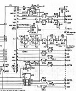
It has a TTL level signal on its pins, it has 14 pins. You can see it named U1 in the centre of this schematic: https://www.dropbox.com/s/zqhgar4g7ib5j4z/Xerox820_FDC_Schematic.pdf

Some pins are labelled on a schematics with:
1=D1, 2=D2, 3=D3, 4=D4,
10=A1, 11=A2, 12=A3, 13=A4, 14=A4,
15=ChipEnable (left to GND),
7=GND,
14=+5Vcc

Thanks

Enrico
 
Wait a second, Enrico--I see that A4 is labeled as pin 14, but then you've said that pin 14 is Vcc. Which is it?

It looks like an inverting buffer to me, but I'll check on the basis that this is a 16-pin IC. Please confirm that.
 
Wait a second, Enrico--I see that A4 is labeled as pin 14, but then you've said that pin 14 is Vcc. Which is it?

It looks like an inverting buffer to me, but I'll check on the basis that this is a 16-pin IC. Please confirm that.
My vote is for a 74S288
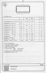
32x8 PROM

(Note that /CE is on pin 15 of this 14-pin IC ;-) )
 
Sorry i was wrong YES the ic has 16 pin.
so it is a PROM? this means that I never can to try to rebuild this interface card?
oh no!! Anybody can help me in any way?
Enrico
 
A prom sounds right.

Check some of the reference designs/datasheets/application notes for the 1791. I suspect that you'll find this design nearly verbatim somewhere.
 
Dear Chuck,
as ever you're GREAT!

Look here at page 12
http://maben.homeip.net/static/S100...sheet/WD Digital FD179X Application Notes.pdf
the FDC 1797 needs to have a RD and a RDclock signals so a way to extract both from the read line input is reported on that application notes.

BUT

i'm not so experto to do this

AND

I expetted that all would be more simple. In this way i have a big works MORE to do.
1) to read very well this application notes;
2) to buy this 74LS288;
3) to understand how to program it;
4) to hope that the codes reported at page 12 would be exact.

If something doesn't works i have not experience to solve this kind of problems.

AND at the last

Also to find this FDC interface card it is not easy:
Who has it he keeps it because he needs it,
Who not knows what it is he simply throws it away.

Thanks SO MUCH!

Enrico
 
My guess is that the circuit in the WD app note was lifted almost verbatim. It's not wise to fool too much with the manufacturer's reference designs!

The 288 requires a bipolar prom programmer--which is uncommon these days. There are circuits that you can built to toggle programming via switches (this is a 32 byte EPROM after all). Finding un-programmed 288s is a bit more of a problem, but they still turn up. You can also program a more conventional GAL that will come fairly close in pinout.

All in all, it's not a brick wall of a problem.
 
Hello everyone, thank you for all the precious tips that are giving me. Something is familiar to me but much more not everything.

I was thinking of replacing the 733W01522 = 74S288 with an eprom 2716, trusting that this small program on page 12 of the application note at the below link https://dl-web.dropbox.com/get/WD D...GKAu9njssXuTScE0iSV_jXqOsoVVxObFu0rvK1SQ&dl=1 would be actually realistic.

I Wonder: could that work? The latency of an EPROM may not be able to correctly read the data from the floppy disk? At the end of the entire circuit (if it works?) has the precisely objective to synchronize data to make them read correctly from the WD1797. In this way the total time disk read will be slightly increased. Is this the only limit their own or instead the controller could not operate?

Enrico
 
Hello Enrico,
doing it with an EPROM is too slow.
Look for an data separator like a WD9216 and it is easy and stable.

Frank
1793_9216.jpg
 
Last edited:
A Xerox 820-II FDC Controller card (it was Chip 733w01522 on a xerox 820-II FDC Cont)

A Xerox 820-II FDC Controller card (it was Chip 733w01522 on a xerox 820-II FDC Cont)

I do not know how much I trust that recopying the code page of the application notes https://www.dropbox.com/s/6b5er8g9uuk42v9/WD Digital FD179X Application Notes.pdf in a 74S288 (82s123 or see the website http://www.hobbyroms.com/proms.html) effectively then i could get a FDC controller working for my card xerox 820-II.

I'd found an alternative that unless typographical errors that I am trying to verify matching the schematic with the xerox schematics), it could be interesting. It is this issue of microcornucopia: https://www.dropbox.com/s/4f8kblogrlzdr9m/FDC_from_Micro_Cornucopia_#22_Feb85.pdf who wrote the article decided to build byself a FDC controller card for xerox 820-II extracting a block of its schematic from a Kaypro-II's one really making very few changes and using a FDC WD1793 + WD9216 separator with external data. Due to its small number of components, and having already a WD1797 i'd need just of a WD9216 (i hope to find it on Internet yet) and wiring it would also be very simple.

What do you think?

Enrico
 
I'd go with the Figure 12 from the datasheet app note. Just have a 288 programmed appropriately. Yes, you can certainly use an 8-pin WD9216 (or equivalent; there is more than one vendor), but you'd have to rework your board to use it. Similarly, you could substitute a WD279x for the 179x and use the internal data separator.

Your choice. It's not rocket science.
 
Hello Enrico,
good news!
In a couple of weeks i receive a Xerox 820-2 with the controller board.
Then i can do a read-out of the data in the PROM.
What do you do with the delay-line U16 on the controller board?

Frank
 
Last edited:
Well, the big problem was to understand what was that U1 chip, then where to find the code to use to program it, then how to program it. Sincerely i was stop myself here. So i not given any look to the delay ic. it is here: https://www.dropbox.com/s/l4wxp3hdsf8s6wb/0447-0400-02.pdf .

I also followed the ebay object 290900473575, but i talked with the seller and he wish to sell the motherboard AND the FDC card togheter. Both are not tested and their price is very high for untested objects. To test them is necessary to have a parallel keyboard, to build a correct floppy cable, to modify the output video to get a composite video, and to create some disckettes with IMD. I done all those things and i'm ready to do this, but i found this schematic https://www.dropbox.com/s/4f8kblogrlzdr9m/FDC_from_Micro_Cornucopia_#22_Feb85.pdf that it seems more simple.
At that time the author pull out the 72 pin card edge connector from the motherboard and he connected the right holes with a new 44 pin card edge connector, then he built the copy of a kaypro-II FDC section schematic. Casually, I have a spare working kaypro-II motherboard so i have not to buy anything than a perfcard like this http://www.ebay.com/itm/ws/eBayISAPI.dll?ViewItem&item=200797705856 that i'm waiting for it to arrive to me in italy. At this moment i checked the schematic on that old microcornucopia's article with the pin of the 72 pin connnector (reported on the xerox 820-II service manual) and with the fdc section schematic of kaypro-ii. I hope to build soon this schematic on that plugboard.


About the possibility to read the contain od U1 it would be fine almost to save that code for history.

Enrico
 
enrico said:
from eMail:
Well: is there a way to read it without desolder it from the ITS PCB?
Hello Enrico,
No, there is no way to read it out in the circuit.
I solder it out of PCB and read the data from it.
Compared to the WD Application Notes it is the same content.

Frank

Here is it:
0000: 01 01 02 03 03 04 05 06 0B 0C 0D 0E 0F 0F 00 01
0010: 01 02 03 04 05 06 07 08 09 0A 0B 0C 0D 0E 0F 00

View attachment FDC820U1.zip
 
Last edited:
Back
Top