• Please review our updated Terms and Rules here

CPD1604S Vertical Collapse

Thanks for the reply Hugo.

If the V POSI signal really is 1.3V (and not 8.3V), the the emitter voltage of Q203 should be about 2V, if it is 8.8v (where you said "okay) then the base-emitter junction of Q203 must be destroyed as it has 7.5V across it in the fwd direction. Check Q202 as well and the fusible resistors.

Base-Emitter on Q203 is like 1.5V on a diode test, and the Base-Collector is a more expected 0.6V. That would suggest it's not behaving correctly. I guess it's toasted.

Not an easy transistor to get, and I can't find anything with the same hFE characteristics in the same maximum ratings. The original transistor is a 2SD1312/2SB984 pair, and they have an hFE of around 200 or so when driven at under 300uA. The highest hFE I can find at such a low current level is around 100 or so.

How important do you think hFE is for this application?

Ow35BUB.png


With all the voltages on Q254 being 24V, this suggests a defect in the V POSI 2 signal, that is supposed to be 7V and instead its 24V, that cuts off Q254 (if the transistor is working), so investigate that too. In the case that Q254 was cut off though, one would expect the collector voltage of it to be lower than 24V, as something should be sinking current to ground in the collector circuit, unless the cause of that fault is a totally shorted out Q254 could explain the measurements.

Probably Q255 is ok, but is base voltage the V Posi signal is simply too low.

There is a slight drop on the collector of Q254, it's 23ish volts and the B and E are 24ish volts. I replaced it with a new part so it (and Q255) should both be fine.


The diodes inside the digital transistor arrays with their cathodes connected to the common rail, normally the power rail, are to prevent the collector voltage of the transistors exceeding the supply voltage. In most cases it wouldn't in a circuit with passive components, but it can if say the transistors are used to drive a small inductive load like a small relay coil it can after the coil is de-energized.

Diodes D608's, D609 are wired as a form of OR logic gate where the diode with the lowest cathode voltage of the three, takes control of the common anode voltage, because by lowering the anode voltage it tends to take the other two diodes out of conduction. So the diode with the lower cathode voltage is the main "controller" of the voltage at the junction of the anodes. For example when D609's cathode gets grounded, it kills the current sourced by the two diodes of D608 and the 10k resistor from the 24V rail to the circuits that D608's cathodes feeds.

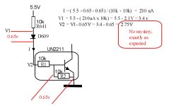
Fascinating. Thanks for the explanation. I really love this kind of stuff and learning about how it all works. That part seems to be working correctly, but the voltage on one of the cathodes inside D609 (D609 is the one with two diodes inside) is too high. The output that leads to Q613 is only 2.7V when it should be 0.1V. I don't think it's coming from D608 though. I think the 2.7V has to be coming from Q613, right?

If only one of the three diodes is supposed to be conducting, then it stands to reason that the output of D608 should only be going to the cathode on the Q615's Base. The other diode inside D608 should be off and not contributing to the voltage on the Base of Q613.

So still then, I don't understand where that 2.7V comes from. Could the bad transistor Q203 be the cause of the lost 6.5V at the Collector of Q613, and that's making 2.7V appear at it's Base? I drew out the voltages on the logic to help myself try to understand what's going on.

There's supposed to be 25V on Pin 11 of IC250. I think this could maybe close the transistor input at Pin 6 and bring it to zero. That closes anodes of D255 and then zero volts appears at Collector of Q612. This causes 6.5V to flow through Base of Q612 and to the collector of Q613 and Pin 1 of IC604. Possibly make sense?

This is what I drew to try and visualize it:

I6hMbrT.jpg
 
Last edited:
So still then, I don't understand where that 2.7V comes from. Could the bad transistor Q203 be the cause of the lost 6.5V at the Collector of Q613, and that's making 2.7V appear at it's Base? I drew out the voltages on the logic to help myself try to understand what's going on.

[/SPOILER]
Don't forget, with a transistor, when all is normal at least, the collector to base junction (which acts as a diode) in the device is reverse biased. Applied collector voltage and any current that might generate does not appear at the transistor's base (except for a tiny reverse C-E leakage current that is insignificant in silicon transistors, but a little more problematic in Germanium ones).

Post the circuit of everything connected to Q613.

Any base voltage you see, if the B-E junction is continuously forward biased should be about 0.6V higher (more positive)than the emitter voltage for a NPN and about 0.6V lower than the emitter for the PNP because of the reversed polarity.

There is the occasional circuit, but it is extremely rare, I have seen the idea used in a video machine control system, it may have been because they had a surplus of transistors, it certainly fools everyone, where a transistor is not deployed as a transistor at all, but a double diode instead. In this case the collector to base junction gets forward biased, the operation as a transistor is not used. Most designers use two diodes or a package with two diodes in it when they need diodes.

Also to expand a little, obviously in switching applications (unlike analog ones), the transistor's B-E voltage could be zero or reversed biased a little at times when the transistor is cut off. However, it is unusual that this would be more than about 5 volts. The reason is that most silicon signal transistors, their B-E junction reverse breakdowns (zeners) at about 7V, and this is to be avoided, because it turns out that if you do that it slowly degrades the transistor's current gain. Though in some circuits you occasionally see a transistor, with its collector not connected and its B-E junction used as a 7V Zener. Some transistors, such as the BC639/640 are unusual in that the B-E junction zeners at around 11v.
 
Last edited:
Don't forget, with a transistor, when all is normal at least, the collector to base junction (which acts as a diode) in the device is reverse biased. Applied collector voltage and any current that might generate does not appear at the transistor's base (except for a tiny reverse C-E leakage current that is insignificant in silicon transistors, but a little more problematic in Germanium ones).

Ok thanks for the correction. I understand I think. However, the missing 6.5V on the collector of Q613 could still be the cause of the 2.7V on its base though, right?

If I think about what you wrote concerning D609/D608, then maybe the lack of 6.5V on the collector of Q613 is causing the diode OR gate to open up on the side toward the base of Q613 when it is not supposed to do so, all because of the lack of 25V on Pin 11 of IC250. Perhaps?


Post the circuit of everything connected to Q613.
This is the areas around Q613 with erroneous voltages noted in red:

KxBVEH0.jpg

This is where the Base of Q613 goes. The other side of D608 just goes straight to the Auto/Manual switch which connects the cathode of D608 to GND or leaves it OPEN. All of the voltages on the other side of D609 are correct as far as I can tell.

b0bIHIo.png
 
A quick check on the information shows that Q613's base voltage is exactly as expected close to 2.7V. Under the condition that the auto-man switch is not connecting D608's cathode to ground.

You might have been chasing your tail, because when that switch is not closed, the 2.7V you are seeing is no mystery at all, it is exactly as one would expect from the circuit values.

You can see how to calculate it attached, you need to calculate the circuit current and allow for the diode voltage drops and the resistances involved.( which as always means you have to look up the device's data sheet, in this case to find out what the internal resistors are in the UN2211).

You don't have to worry about the 10k base to emitter resistor R2 in the UN2211, because it only takes about 65uA to get the B-E junction to conduct and that stabilizes the B-E voltage at around 0.65V simplifying the calculation. With Q613 biased on, as it is, one would also expect its collector voltage to be close to zero that you measured.

Maybe you should move back to the pincushion circuit to find out why the emitter follower there was misbehaving.
 

Attachments

  • Trans.jpg
    Trans.jpg
    87.6 KB · Views: 3
You might have been chasing your tail, because when that switch is not closed, the 2.7V you are seeing is no mystery at all, it is exactly as one would expect from the circuit values.

Oh no! If that's the way it's supposed to be, that means the voltage readings are supposed to be taken with the switch in the "manual" position!

I guess I assumed it didn't matter where the switch was because the Service Manual absolutely does not tell you where the switch should be for the voltages and waveforms in the schematic. All it says is "color bars pattern" and "31.4kHz, 70Hz."

Thanks for pointing that out, I might have continued trying to "solve" this for a long time!

Maybe you should move back to the pincushion circuit to find out why the emitter follower there was misbehaving.

Definitely want to, but Q203 still needs to be replaced. I'm 100% sure it's bad as it reads very off and also the Vertical Position control doesn't work at all with it installed so there is that. I think maybe Q203 was weak and going bad slowly. It connects to the 24V supply, so it easily could have been damaged before I got to the set as it was the 24V supply which had a bad fusible resistor.

I am hoping that the mismatched assortment of voltages present in the logic surrounding !C250 and IC302 is the cause of issues in the Pincushion circuit. I am prepared for the problem to remain and continue working on it, but the Vert Position Signal does connect to Pin 2 on IC304 (through Q255), which is one of those two Pins that are responsible for generating the missing parabola on Pin 7. Even though I'm seeing the correct 2.2V on the base of Q255, perhaps it's somehow effecting the current to Pin 2?

Either way, I'd have to put the broken transistor back onto the PCB in order to continue testing, and I'd be worried about making something worse.

Speaking of which, I can't find the 2SB984K transistor anywhere on internet at all, not even a whisper. I purchased the ZTX751/ZTX651 PNP/NPN pair to replace it with, hopefully they are okay. The biggest difference I can see is that the original transistors have a much higher voltage tolerance (VCBO 120, VCEO 80) than my chosen replacement (80V, 60V respectively), but it seems like this spot in the circuit would never see more than 24V anyways? The hFE and fT characteristics are pretty similar. The pinouts are unfortunately different, but I take care of that by rearranging the legs a bit I guess.

CyFpgdb.png

SbM8vEu.png
 
I replaced Q202 and Q203.

Voltages are now correct in that whole area of the board. The base of Q255 is 8.3V exactly. All of the Size and Position controls are working correctly and as expected. I followed through the Service manual and did a rough setup of the raster sizes and positions and those things look more or less correct.

The pincushion controls still do not work as expected. My raster is still bowed and messed up.

However, I now have a parabola on Pin 7 of IC303.

kCjS9WI.jpg


Service Manual says my Parabola should be only 0.5Vpkpk, but I have ~1Vpkpk, not including the extra background information. It seems 2X too high?

bJfs9P3.png

Raster is still messed up:
BIdnc2p.jpg

I am looking around for anything out of the ordinary and I found that there is some behavior I can't explain. In the Side Pin control circuit, the collector of Q312 did not have the voltage as called out in the service manual. It says 9.0V, but it was around 5V. I found that the voltage at this spot will fluctuate between about 4-12V depending on how I set the side Pin controls. I am not sure if this is correct behavior, but I thought it was possibly wrong.

p1z7Bed.png
 
Last edited:
By adjusting the DC voltage on Q312's base, with the side pin presets, this controls the gain of the differential amplifier of Q312 and Q313 and also causes a DC offset of the collector voltage of Q312 which is expected. The DC offset part, varying between 4 and 12V is ignored by the emitter follower Q315 because the signal is AC coupled to its base by C334.

Can you scope the base and emitter of Q315, because previously the result was abnormal.
 
By adjusting the DC voltage on Q312's base, with the side pin presets, this controls the gain of the differential amplifier of Q312 and Q313 and also causes a DC offset of the collector voltage of Q312 which is expected. The DC offset part, varying between 4 and 12V is ignored by the emitter follower Q315 because the signal is AC coupled to its base by C334.

Okay, thanks for the explanation. That makes sense; I have definitely come across other situations with schematics where they just give a "nominal" value and expect you to know it going to change with an adjustment.

Can you scope the base and emitter of Q315, because previously the result was abnormal.

The collector of Q315 is a flat 12VDC.

pEEQtEH.jpg


The Base of Q315 has the sawtooth wave at about 2V above zero, with an approximate peak to peak of about 1.8V (only measuring the solid white part of the wave and ignoring the translucent fuzzy part).

gmQs47t.jpg

The Emitter of Q315 has the sawtooth a little lower at about 1.7V, but the waveform is larger at about 2V peak to peak (only measuring the solid white part of the wave and ignoring the translucent fuzzy part).

vFZfFTV.jpg

Looking at what the schematic has to say, the Base of Q315 is suppose to be about 2.8VDC measured, and the Emitter is supposed to be about 2.2VDC; they both measure correctly. Looking at the waveforms I captured for the Base and Emitter, they both have an RMS voltage on the scope that closely tracks with the DC voltages on the schematics. They are a little high (Base is 2.98VRMS VS 2.8VDC, Emitter is 2.38VRMS VS 2.2VDC), but I would generally tend to assume that's a reasonable margin of error? If the waveforms I captured had a significantly higher DC offset or pk-pk value, I would think the DC voltages would end up much higher than the schematics say they should be? Perhaps I'm missing something.


NbmaL0S.png
 
It looks much better than before. This improvement happened after you cleaned the pcb and replaced some parts. It is almost correct. The pp amplitude of the sawtooth on the emitter needs to be about 2.5 to 2.6Vpp. See if its amplitude comes up a little when you adjust the side pin presets or RV313.

When that is correct, scope around IC303 again so we can check that is working, after that we will follow its output pin 5 and find out why its not actually correctly the sides of the raster scan. For the output of IC303, measure it again with the R-C filter (because its a PWM signal).
 
It looks much better than before. This improvement happened after you cleaned the pcb and replaced some parts. It is almost correct. The pp amplitude of the sawtooth on the emitter needs to be about 2.5 to 2.6Vpp. See if its amplitude comes up a little when you adjust the side pin presets or RV313.

There's nothing that seems to make the sawtooth on the emitter of Q315 bigger. If I turn the Pin Up to the right, it will pull the square wave down a bit in a funny squiggly way, but it doesn't make it taller. The Side Pin controls don't seem to do much of anything at all. The only action I can get out of the Side Pin controls is if I turn them down all the way (either one of them), the Sawtooth disappears completely.


When that is correct, scope around IC303 again so we can check that is working, after that we will follow its output pin 5 and find out why its not actually correctly the sides of the raster scan. For the output of IC303, measure it again with the R-C filter (because its a PWM signal).

Can't do it. Nothing makes that waveform bigger, and the Side Pin controls don't have any effect on the sawtooth other than to extinguish it completely.
 
Last edited:
I found an area that seems off. Q310 has blown up three times now, and I thought it was because of something I did wrong, but now I'm starting to think it might be the result of something else.

I found that the voltages on Q309 were too high. The Base and the Emitter are supposed to be around 12V and 15V, but they are both about 17V.

Also, the 20.6V which is supposed to be on the shunt regulator IC304 is at ~22.6V. The other side of the regulator responds to adjustment and is stable at 2.5V, but the 22.5V doesn't change at all.

I guess I'm most concerned with the high voltages around Q309 and the fact that Q310 keeps blowing open.

ocWvzos.png
 
What is the base voltage and collector voltage of Q310 on testing ?

Will adjustment of RV314 bring down the base and emitter voltage of Q310 to the correct value ?

I think the job of the Zener D311 is to prevent the collector to base source voltage of Q310 being exceeded, is that Zener ok ?
 
What is the base voltage and collector voltage of Q310 on testing ?

It was testing at 17V on the Base and 24V on the Collector.

Will adjustment of RV314 bring down the base and emitter voltage of Q310 to the correct value ?

No, it did not. I decided to replace IC304 because I got a couple of them.


I think the job of the Zener D311 is to prevent the collector to base source voltage of Q310 being exceeded, is that Zener ok ?

D311 was not fitted from the factory. I actually purchased the exact diode (still available), but I didn't fit it because I thought they must have left it out for a reason?


OK. So I went and just replaced IC304 and that gave me adjustability of the 20.6V back. The voltages around Q310 and that area are now at ~15V as they are supposed to be, I now have some Pincushion controls!

I'm not sure that it's really working correctly now, but the Side Pin controls are finally doing something. I will have to go through all the setup stuff again with each resolution and do the free running frequencies and stuff again and see what it looks like.
 
good progress !

Thanks!

So I spent some time messing around with the controls and I also replaced IC303 and IC301 with NOS ICs and that cleaned it up a little bit more. Not 100% perfect, but very close to, to the point that I think it's convergence or it just needs a couple magnetic strips.
 
Last edited:
Finally got it back in the case, and I had a minor hiccup. One of the capacitors on the DA had broken a trace and it stopped working again.

After three and half hours, I tracked down the problem and set it right again. When I finally got it in the case and looked at it straight on a desk, I realized that the yoke is misaligned. I went in and freed up the goo and twisted it a little to correct for unevenness, but when I got it together again, it became apparent that the yoke it point up a tad bit (or is it down?)

This is a big exaggeration, but it's bowed upward a tiny bit like this:

bent.PNG

And I can tell it's a yoke issue because the convergence is off in a pattern that reflects the bow.

Not sure if this is a result of the shipping or what, but the glue and everything on the yoke is very well attached from when it was last serviced by Sony, so that would suggest to me that it was misaligned at that time.

Luckily (I think it's lucky), the tube seems to be one that got replaced later on it's life as there is zero burn-in and it has later date codes than the monitor itself. It's also getting above peak stated nits during setup procedure, so I think it's fairly minty.

Unluckily, when it got swapped by Sony, they did a bad job aligning it. I guess since it was being used in a CNC shop, they didn't think anyone would really care.

I'll have to go in and point it right, and probably do a full purity and ring alignment, which I was hoping to avoid.
 
I had to go in and remove all the yoke wedges and start over. whoever replaced the tube did a really bad job of it and all the convergence adjustments and such were messed up.

After doing beam landing, static convergence, dynamic convergence, white balance and geometry, it now looks pretty good.

There is one thing left that's bothering me though. During the setup instructions, it tell you to display a crosshatch pattern and to use the G2 to produce a back raster, and then to center the back raster horizontally with the rough adjustment on the main PCB while in a 57kHz mode.

I did this, but I can see the side of back raster looks to have a different geometry from the crosshatch image displayed on top of it. Specifically, the Pin Phase looks like it's kind of opposite between the back raster and the overlaid image. I adjusted the Pin controls on the DA board to make the image look best of course, but it strikes me as odd that they are different.

I don't believe that it has anything to do with the yoke because I set that up for best purity and so that the top and bottom of the image are straight across. If I was to try and correct the back raster with the yoke, it would have a droop or a bump on the top and bottom.

Maybe it's just supposed to be like that? Has anyone ever run across a monitor like this and know how it's supposed to be setup?

Anyway, this is what I have now. I think it's pretty darn good:

ilElBDI.png
 
That looks pretty good to me. These monitors were never perfect, but our eyes have become used to the perfect geometry of an LCD. Tilting the yoke affects both the bowing of horizontal lines as well as the convergence. You have to pick the best compromise.

I'm not surprised the CRT was replaced. Back when these were still fairly new, I saw a LOT with weak blurry CRTs. In fact, I'm not sure I ever saw one with a good picture. Sony must have had a defect in their 16" CRTs since the other sizes were fine.

Yeah, it's not bad at all, but I do think there is still something a little odd going on. When I turn it on after it's been sitting, the horizontal width will bounce in and out a little bit until it warms up. I'm not totally sure what that's about, but I noticed awhile back that the 12V supply looks a bit low at around 11.7V.

With this continued strange behavior, it got me thinking that the regulator might have been weakened by whatever calamity took out the 24V fusible resistor. As you can see, there's supposed to be 12.3V on the other side of the 7812, but there is 11.7V, which seems maybe just too low?

I have a new 7812 in the mail, but I wasn't immediately able to figure out a good replacement for D904, the SB50-09J, so hopefully that's fine (even if it wasn't at 15.6V, I think the 7812 would just keep its output steady at ~12V, right?). Also of course not sure if the 7812 is the problem, but all the electrolytics have been tested and any bad replaced, so I can't figure what else might be to blame.

lDH7Zb6.png
 
Last edited:
It is interesting with 78xx regulators, in that over time they tend to have a small voltage shift in the downward direction, never up it seems.

That circuit probably measures just over 12V (12.3) at the regulator output pin with respect to GND because of the small voltage drop across the 0.45uH L909, L912 inductors and after L905 is drops a little again to 12V. Interesting that the current return via those two inductors is proportional to that in the +24 and +78V and +160V supplies. The DCR of the two 0.45uH chokes must be very low.
 
Last edited:
Back
Top