Hugo Holden
Veteran Member
looks fine.Ahh... sorry about that. The diodes were a bit difficult to discern. One more for review... I'll upload the gerbers when you give the okay.
View attachment 1278722
looks fine.Ahh... sorry about that. The diodes were a bit difficult to discern. One more for review... I'll upload the gerbers when you give the okay.
View attachment 1278722
Good idea to cut up some sacrificial plate I think. Only get the one chance with the real box.
One thing, I do not have the actual switches yet. It will pay to measure those switch bodies, just in case the dimensional drawing we found is not ideal.

Does it not seem the space between solder pads for C4 is little more than a hair's width - ie unnecessary close together?Attached are the gerbers for the JS-1 board. I added some identification text, and filled in the junctions at C5 and Q1. No problem making revisions at any point, just let me know.
View attachment 1278737
I found the springs that work.
The wire size is 0.4mm
The length is 15 mm
and the diameter 4mm
They come in a 10 piece pack.
They are available here, they need to be selected from the options:
0.3-3mm Stainless Steel Spring Expansion Extension Tension Springs 10-300mm Long | eBay
Lengthï¼10~300mm. Material: 304 Stainless Steel. Quantityï¼1/2/5/10 Pieces.www.ebay.com
Does it not seem the space between solder pads for C4 is little more than a hair's width - ie unnecessary close together?
") .
.Agree - the pad sizes could be made much smaller. They look to be twice as large as necessary.They are close together, but when scaled the pad sizes seem to match the original jpg that was uploaded. I should probably reduce the pad sizes on that one (indeed, all the component pads are a bit larger than I would personally use).
Hugo: the pad sizes I came up with by scaling your original jpg to the specified board size are as follows:
external connection pads: 3.5mm
regulator and c5: 3.0mm
Most of the other components looked to be 2.65mm, with a few at 2.75mm (ie. diode D4). Not sure if that was due to the jpg DPI, scaling, or my vision
Happy to change them to whatever... feedback welcome. Thx.
Agree - the pad sizes could be made much smaller. They look to be twice as large as necessary.
I am following the discussion with great interest, and am also acquiring the parts to build a couple of these controllers.

These look great! I'll DM you about shipping.I've added the DXF for the front panel to this zip, let me know if you have any comments.
Let me see if I have any 6061 sheet in stock, I can do a test cut. I just did a bunch of updates to the CNC machines so they aren't fully proven yet, so I'll likely do several proof cuts before going after the final box.
If I'm reading the datasheet right the thickness of the top panel on the box is 060, which is refreshingly thin.
This looks much better to me. Thanks for doing this! Any way we can label the input pads now that there's a little more room?I intend to build a couple of these as well... very neat project. So here is a variation with pad sizes that are a bit more suitable from my perspective. All component pads are 1.8mm with the exception of the regulator and the 4 link pads, which are at 2mm. All hole sizes are per Hugo's specification. It's up to the group how to proceed, just let me know and I'll adjust if required and produce new gerbers.
View attachment 1278753
Another thing that does not look right is the amount of space between the mounting screw hole for REG1 and its three solder pads. Based on the available lead for these TO220 regulators, the farthest distance between the mounting screw hole and any of the solder pads should be 3/4". Use the footprint for the regulators on the Dazzler board as an example.I intend to build a couple of these as well... very neat project. So here is a variation with pad sizes that are a bit more suitable from my perspective. All component pads are 1.8mm with the exception of the regulator and the 4 link pads, which are at 2mm. All hole sizes are per Hugo's specification. It's up to the group how to proceed, just let me know and I'll adjust if required and produce new gerbers.
View attachment 1278753
Nitpicking but could you modify this trace to avoid an acute angle?
View attachment 1278761

None of the positions of the board pads are particularly critical, except perhaps a little for the 7812.
One reason large pads are used is that the prototype boars of the single side I made (like an old fashioned board) and home etched are better off with large pads as there are no plated through holes to give them strength. If you look at single sided boards of yesteryear, they always had relatively larger pads compared to modern boards.
You could shrink the pads on a modern board version with plated through holes, if you wanted, but I think they are fine as they are, if you scale the board to real size they really are just right as they are. Many modern boards the pads are not a lot bigger than the track thickness and the tracks are super thin, it really is not a good idea, especially of one day parts require de-soldering and replacements.
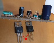
For the 7812, when it sits flat as it does in this case, be aware that there are two versions of it, see attached photo. Some specimens have a longer section on the lead wires as they exit the case, and this version has to be allowed for. If the holes for the leads are spaced too close to the mounting hole in the tab, they don't fit properly. Or if the holes are too far away the leads don't reach. So despite what you read about the 7812 package, the holes were specifically placed to work for both regulator types.
And just a note on mounting small glass diodes vertically, always leave at least 5mm of lead wire to sit the diode body above the board surface, otherwise the lead is too short and there is more thermal and mechanical stress on the diode body where the lead enters the package.
It is a good idea to have plated trough holes and pads on both sides and the +12V supply link could be a track on the top surface. The other link probably better left as a link wire, in case a resistor needs to go there.So at the moment, I have the holes plated through. Apologies if I missed it, but is there a specific reason as to why they shouldn't be?
Re. the regulator footprint, I actually have the holes a few mils further from the body than the standard package footprint used by my software. I can put them wherever, but perhaps we should use aligned pads vs. using a staggered ground pad?