• Please review our updated Terms and Rules here

Diagnosing which RAM chip is faulty

Flamin Joe

Experienced Member
Joined
Jul 24, 2013
Messages
176
Location
Brisbane, Australia
Hi guys. I've got a problem with my Atari PC3 8088 in that I would get a "divide overflow" error when trying to run certain programs or in some cases it would simply lock up the PC. I've already had a faulty RAM chip which has been replaced, so suspecting more faulty RAM chips I ran a program called RAMTEST 2.00 by Brown Bag Software. It was the only small sized RAM test program which would run, anything too large in size (50k or more) would also cause lockups. Anyway this is what it came up with:

https://plus.google.com/u/0/photos/...lbums/5950521323764912161/5950523540717012962

Base memory read error at address 70002
This address is in the 8th 64k bank of base RAM (2nd 256K bank)


Now back when I had a PC like this I never really tinkered around with the hardware much besides installing a sound card. It wasn't until the 386/486 days and SIMM memory that I really started delving into things like this. So while not being a computer noob by any stretch of the imagination, I sure do feel like one trying to get my head around this. :D From what I gather from this wiki page: http://en.wikipedia.org/wiki/Conventional_memory the RAM location it reports is the "Ordinary user memory to 512 KB".

Here is the board in question and it's memory chips all conveniently soldered in so just swapping chips around or easily replacing them is out of the question!

https://plus.google.com/u/0/photos/...lbums/5950521323764912161/5950521324510791154

Note: The chip at U90 has already been replaced. The system when I first got it was only reporting 576K of memory at boot up and after "piggy backing" a replacement chip over the top I found it to be the culprit. It now reports all 640K.

I have replacement chips for the both the Sharp LH2464-12 and the Siemens HYB 41256-12 but using the "piggy back" method it still reports a memory error. I'm guessing this method only works for dead chips?

Would appreciate it greatly if someone could point me in the right direction or at least narrow it down. Thanks.
 
Ok thinking about it a bit more and doing further research I think I might be getting my head around it. I assuming the "2nd 256K bank" is referring to one of the 4 Sharp LH2464-12 chips which I know are 256K. Also if I'm correct, the "8th 64k bank" being at 512 KB falls within those 4 chips as together they make up the RAM between 384K and 640K.

Now being that the RAM chips are not in order on the board, I assuming it goes by reference number not physical location? So for example U87 (1st 256K bank), U88 (2nd 256K bank), U89 (3rd 256K bank) and U90 (4th 256K bank)? That makes sense to me since U90 was the dead chip I replaced hence I was only getting RAM up to 576K (U90 would have made up the last 64K to 640K).

So after all that, I assuming U88 is the faulty chip? After typing this all out it's making complete sense now. :D I guess I'll find out later when I get home and replace the chip!
 
No, because a 'dead' chip might, for example, be always driving its output high (or low), something that piggybacking will not be successful with.
Just accept that piggybacking only works some of the time.
Some other reasons for piggybacking not working are listed at http://www.minuszerodegrees.net/5150/ram/5150_ram_piggybacking.htm

Thanks for sharing I'll keep that in mind.

Well I'm no closer to finding the faulty RAM chip. :( Replaced the chip at U88 and it still reports the exact same memory error. So I went ahead and also replaced U87 and U89 and it's still the exact same error. So I'm back to square one scratching my head as to what chip is at fault. Could of sworn I was on the right track unless the memory tester is not reporting the location properly? Like I mentioned earlier, I've been unsuccessful in trying to find another program which will do the job as anything too large would lock up the PC trying to run it. This is the only one I've found so far which would run and allow me to perform tests.

I don't have enough spares to replace all the Siemens chips so if it is one of those I can't do a blanket replace them all to fix the problem. So I need someway of narrowing down to at the very least which row it is. Any pointers?
 
This address is in the 8th 64k bank of base RAM (2nd 256K bank)
RAMTEST (or any other diagnostic) cannot interrogate the 8088 based motherboard to establish bank size, so the line above is simply RAMTEST trying to be helpful. To some, it will be more misleading than helpful.

Your pictured RAM is:

16 x HYB41256
The datasheet indicates that each chip provides 256K by 1 bit
Therefore the 16 x HYB41256 provide: 16 x 256K x 1bit = 4096 Kbit = 512 KB
The 512 KB will be wired as two 8-bit banks of 256 KB.

4 x LH2464
The datasheet indicates that each chip provides 64K by 4 bit
Therefore the 4 x LH2464 provide: 4 x 64K x 4bit = 1024 Kbit = 128 KB
The 128 KB will be wired as two 8-bit banks of 64 KB.

As for bank numbering, the situation is most likely:

Bank 0: 0 to 256 KB (8 x HYB41256)(256 KB in size)(8 bits wide)
Bank 1: 256 to 512 KB (8 x HYB41256)(256 KB in size)(8 bits wide)
Bank 2: 512 to 576 KB (2 x LH2464)(64 KB in size)(8 bits wide)
Bank 3: 576 to 640 KB (2 x LH2464)(64 KB in size)(8 bits wide)


Base memory read error at address 70002
70002 hex = 448 K
So the faulty chip is the bit 6 one (as displayed by RAMTEST) in bank 1 (the second bank).

The problem you have is that the motherboard is not labeled as to which chips are in which bank, and within each bank, which chip corresponds to which bit. Physically, the HYB41256 chips could be in any kind of order. I think you need to find a technical manual?
 
The problem you have is that the motherboard is not labeled as to which chips are in which bank, and within each bank, which chip corresponds to which bit. Physically, the HYB41256 chips could be in any kind of order. I think you need to find a technical manual?

If it's any help, I actually have the schematics for this motherboard which I picked up from an Atari dealer in the US a while back. I've done a quick scan of the RAM but since the sheets are quite big so I could only scan a bit at a time. I've scanned what I think is the most relevant part for now which shows it in some sort of arrangement.

https://plus.google.com/photos/107273536606018845980/albums/5950521323764912161/5952024505898242850

There's no markings anywhere saying which bank is which however it does appear to suggest that U51, U52, U53, U54 and U64, U65, U66, U67 are part of one bank (they are marked 0 to 7) and U73, U74, U75, U76 and U82, U83, U84, U85 are apart of another bank (also marked 0 to 7). I assume going by the numbering and their positioning on the schematic that they are Bank 0 and 1? I'm also assuming that would then make U87 and U88 Bank 2 and U89 and U90 Bank 3?

70002 hex = 448 K
So the faulty chip is the bit 6 one (as displayed by RAMTEST) in bank 1 (the second bank).

So taking into account my assumptions above, U83?
 
Unfortunately, the addressing circuitry is not shown in the image that you provided.
I agree that those numbers that you refer to are the diagram's author indicating the bit number.
Those numbers together with what CAS/RAS lines are being shared among the chips reveals:

Bank ? (256 KB) = U51:bit 0, U52:bit 1, U53:bit 2, U54:bit 3, U64:bit 4, U65:bit 5, U66:bit 6, U67:bit 7
Bank ? (256 KB) = U73:bit 0, U74:bit 1, U75:bit 2, U76:bit 3, U82:bit 4, U83:bit 5, U84:bit 6, U85:bit 7
Bank ? (64 KB) = U87:bits 0/1/2/3, U88:bits 4/5/6/7
Bank 3 (64 KB) = U89:bits 0/1/2/3, U90:bits 4/5/6/7

We know about bank 3 because your earlier replacement of U90 affected RAM past 576 KB.
It makes sense that the remaining 64 KB bank is bank 2.

But we don't have enough information to determine banks 0 and 1. So at this time, the faulty bit 6 chip could be either U66 or U84. If you provide an image of the circuitry that generates the CAS and RAS lines, then we should be able to determine which 256 KB bank is 0 and which is 1.
 
Here's the part showing the RAS and CAS lines. Sorry for the bad scan but it's hard to get it right when your trying to scan such a large document into a smaller scanner all without trying to damage it.

https://plus.google.com/u/0/photos/...lbums/5950521323764912161/5952257730869463250

So I take it that the RAS0 and CAS0 lines going to the top bank indicates that it is indeed Bank 0? And the corresponding RAS1 and CAS1 lines going to the second bank indicates it is Bank 1?
 
So I take it that the RAS0 and CAS0 lines going to the top bank indicates that it is indeed Bank 0? And the corresponding RAS1 and CAS1 lines going to the second bank indicates it is Bank 1?
Not necessarily. Per below, the same signals also go to banks 2 and 3.

Bank ?: U51/U52/U53/U54/U64/U65/U66/U67 = CAS0 / RAS0
Bank ?: U73/U74/U75/U76/U82/U83/U84/U85 = CAS1 / RAS1
Bank 2: U87/U88 = CAS1 / RAS0
Bank 3: U89/U90 = CAS0 / RAS1

If I had to bet which of the two 256 KB banks in the diagram is which, I would bet bank 0 for the top one, and bank 1 for the bottom one, but I've been caught out before.
We really need to see the circuitry that generates the CAS and RAS signals.
 
Alright I decided to take a punt and go ahead and replace U84 figuring if it wasn't that I can always then replace U66 since I have enough chips to do so. Result, now I'm getting no post or display. :( I double checked the solder and everything seems to be fine. I even redid it the soldering just in case but no difference. Thinking I may have got unlucky and the chip I replaced it with was faulty, I then desoldered it and put another one but no change. I also did a quick check with the multimeter and it all appears to be good. Never had a an issue when I replaced the other chips. :confused:

Does the RAM have to be an EXACT match, and I'm talking an exact match right down to the manufacture date? It's the exact same part number but the date code on the original RAM is either 8916/8912 where as the "new" RAM I have is much later in the year being 8942. Just took a quick pic:

https://plus.google.com/u/0/photos/...lbums/5950521323764912161/5952758023397293394

Didn't notice this before until I put them side to side, but the original chip is slightly larger as well. Different print alignment as well all pointing to a different factory I assume. I wouldn't think it would be an issue unless these older boards are more picky?

Either way if I get time tomorrow night I'm planning on removing the replacement chip and putting the original one back in. If it starts posting again then that will answer my question!
 
Alright I decided to take a punt and go ahead and replace U84 figuring if it wasn't that I can always then replace U66 since I have enough chips to do so. Result, now I'm getting no post or display. :( I double checked the solder and everything seems to be fine. I even redid it the soldering just in case but no difference. Thinking I may have got unlucky and the chip I replaced it with was faulty, I then desoldered it and put another one but no change. I also did a quick check with the multimeter and it all appears to be good. Never had a an issue when I replaced the other chips. :confused:
Of the PC family, many motherboards will not POST (they will appear 'dead') if a chip in bank 0 has completely failed. Maybe your Atari is the same. If so, then maybe the bank that U84 is in is bank 0, and your replacement chip is faulty.

Does the RAM have to be an EXACT match, and I'm talking an exact match right down to the manufacture date?
No.

It's the exact same part number but the date code on the original RAM is either 8916/8912 where as the "new" RAM I have is much later in the year being 8942. Just took a quick pic:

https://plus.google.com/u/0/photos/...lbums/5950521323764912161/5952758023397293394

Didn't notice this before until I put them side to side, but the original chip is slightly larger as well. Different print alignment as well all pointing to a different factory I assume. I wouldn't think it would be an issue unless these older boards are more picky?
No. I am very sure that something else going on. The reason I gave earlier is a plausable expanation.

Either way if I get time tomorrow night I'm planning on removing the replacement chip and putting the original one back in. If it starts posting again then that will answer my question!
I'm guessing that you are now wishing you had soldered in a socket.
 
Ok things are just going from bad to worse now. I thought I found the problem after removing the replacement chip as I noticed one of the solder pads on the PCB was missing. I must of missed it when I quickly checked it last night and testing it with my multimeter confirmed there was indeed no circuit. Managed to repair it and ended up putting in another replacement chip just in case the last was faulty. Confirmed once again with the multimeter there was now a circuit but still no go. So I decided to put back the original chip in thinking maybe I received a batch of dodgy RAM, tested it once again with the multimeter before powering on, still no go.

Apart from that one pad, everything else looks fine, but I fear all this desoldering/soldering of the same section is just going to cause further damage. I've replaced other RAM chips, even put in a socket for the CPU so I could upgrade it to a V20 which worked a treat, so it's not like I don't have experience. But something is not going right here and I'm at a loss to explain it right now.

I think I'll give it a rest for now and maybe come back to it at a later date and do a more detailed examination. There must be something I'm missing but right now I've had enough of looking at it. I was hoping I wouldn't have to but worse case scenario I'll just have to use my backup board which works perfectly.

I'm guessing that you are now wishing you had soldered in a socket.

lol yeah something like that! Fortunately before I started doing all this I invested in a Hakko 808 Desoldering Gun which makes light work of removing solder. If I'm feeling adventurous later, I might just start a fresh and remove all the chips replacing them with sockets to make things easier. It would fit in with what I'm trying to do with this board, making it a "supercharged" lol Atari PC3 motherboard with a few minor upgrades. :)

Thanks for all your help modem7 it really has been appreciated. :thumbsup: One of the things I wanted to do besides reminisce playing around with my very first PC, was to learn more about how these older PC's ran under the hood. I've definitely done that with all the knowledge you've shared. Thanks again!
 
I already thought the same.. Soldered memory isnt very pleasurable..
 
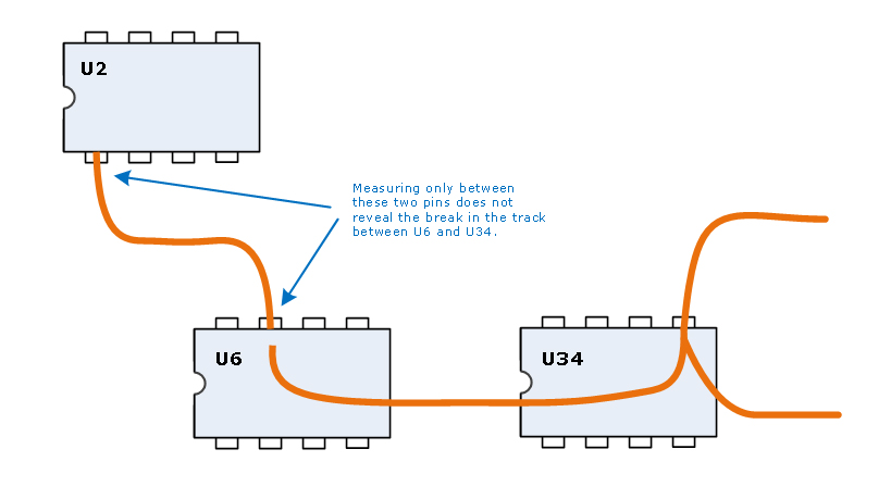
Confirmed once again with the multimeter there was now a circuit but still no go.
In case you are not already, be aware of the following trap:
break_in_track.jpg
 
Thanks for reminding me it's provided me with some inspiration to check things over again but I'm still no closer to a resolution. All the tracks across all RAM chips appear to be fine and I confirmed it by comparing it with the working board I have.

My only thought is that perhaps I've somehow managed to kill one of the other chips hence it will now not post. :confused:

Anyway I'm kind of warming to the idea of removing all the chips to replace with sockets at a later stage and perhaps even going as far as replacing all the chips with a "fresh" batch. Seems like a pretty drastic thing to do but with the issues this board has had with RAM, it might be a worthwhile project.

Just on the question of RAM if I went the all out replacement route, does it need to be the same speed as the original stuff? I know the HYB41256-12 is a 120ns part but I noticed on my spare working board (which is a year earlier revision) that it has NMBS AAA2801P-10 chips. I assume it would just run at the lower speed much like RAM does today? I'm curious because the difference in these two boards is quite noticeable, it's not just a small revision. Apart from a different PCB colour, it also has a few different chips and some are socketed on the older board where they aren't on the newer board and vice versa. A good example is the HD74S51P just above U90 which is socketed on the newer board, yet on the older board it is a 74S51N and it is soldered.

Anyway I'm rambling on I just wondered if that would make a difference. If I could stick the faster RAM on it (not that it would make much of a difference) I think that would be good and fit with what I'm doing to the board. :)
 
Just on the question of RAM if I went the all out replacement route, does it need to be the same speed as the original stuff? I know the HYB41256-12 is a 120ns part but I noticed on my spare working board (which is a year earlier revision) that it has NMBS AAA2801P-10 chips. I assume it would just run at the lower speed much like RAM does today? I'm curious because the difference in these two boards is quite noticeable, it's not just a small revision.
The speed rating of the chips is the fastest that the motherboard should run the chips at. These old RAM chips cannot be interrogated for specifications by the motherboard, and each of your motherboards will be running whatever chips are fitted at a fixed 'speed'.
The best analogy that I can think of is the speed rating on your car's tyres. Putting on faster speed rated tyres does not make your car go faster - the engine and gearbox will still be turning the wheels/tyres at the same speeds.

Modern computers are different.

Apart from a different PCB colour, it also has a few different chips and some are socketed on the older board where they aren't on the newer board and vice versa.
Even with the IBM PC, there are visual variations between motherboards.

A good example is the HD74S51P just above U90 which is socketed on the newer board, yet on the older board it is a 74S51N and it is soldered.
Both are 74S51 chips, but of different make. The 'HD' prefix of HD74S51P tells me that the chip is made by Hitachi. If I was to look at the chip's data sheet, I would probably find that the 'P' suffix is Hitachi indicating a plastic case. Similarly, the 'N' suffix of 74S51N is probably its maker's way of indicating a plastic case.
 
At some point, you may need to create some ROM based code
that doesn't depend on RAM to run. Used in combination with one
of those boot status boards could be the way to go. The 8088 is
relatively easy to write code for at the lowest level.
Don't assume that because RAM fails that it is the RAM itself
that is at fault. There are buss buffers, address muxs, refresh and address
decoders that can cause RAM to seem to fail.
Dwight
 
Back
Top