• Please review our updated Terms and Rules here

Five Festive 5150 Boards (BOARD #1 Thread)

It is starting to feel like U9 is bad isn't it
If we just look at A13 (for the procedure), crudely:

1. 8088 takes its A13 pin to HIGH, and sets its three status pins to indicate a memory read operation.
2. The 8288, seeing a memory read operation, knows that the 8088 has outputted an address, and accordingly, the 8288 pulses its ALE pin.
3. That positive going pulse causes U9 to sample its pin 7 (connected to the 8088's A13 pin) and put that into a latch within itself.
4. With U9-1 being LOW, that gets U9 to output the aforementioned latch output out onto pin 6.

But I can put most of that aside.
If I look at the datasheet for a 74LS373, pin 1 being low takes the outputs out of high impedance state - the outputs should be either HIGH or LOW.
You are not seeing that for the output corresponding to A13.
U9 at fault, or affected by something on the address bus ?
 
1. 8088 takes its A13 pin to HIGH, and sets its three status pins to indicate a memory read operation.
2. The 8288, seeing a memory read operation, knows that the 8088 has outputted an address, and accordingly, the 8288 pulses its ALE pin.
3. That positive going pulse causes U9 to sample its pin 7 (connected to the 8088's A13 pin) and put that into a latch within itself.
4. With U9-1 being LOW, that gets U9 to output the aforementioned latch output out onto pin 6.
That's cool that you can break it down like that. The 8288 and 5150 bus protocols in general are still a bit "too big" to fit in my little brain haha. With enough practice and hands-on maybe I'll get there, and thanks to your help and all the concise materials on your site it's slowly sinking in :)
 
Ok, I replaced U9 with known good. We're a lot closer now. All bits salute except for A11 which is now at a high impedance state, where before it was low.
 
Oh darn, never mind. I thought it wasn't connected but must have been a slip on the multimeter. Connectivity between the ISA slot and U9 is solid.

Shame this last address line A11 is hung. Could be tricky to track down. Will pick it up tomorrow.
 
I'm assuming another chip on the bus is hanging A11. According to [this diagram], candidates are:
  1. U62-13 / LS158 / RAM Multiplex
  2. U15-8 / LS244 / External Address Bus Driver
  3. U18-9 / LS373 / DMA Address Latch
I'm going to try the IC piggyback where I can to revive the signal as it's less destructive than leg snipping.
 
Last edited:
I'm assuming another chip on the bus is hanging A11
Keep in the back of your mind that the known-good U9 that you fitted may not actually be fully functional. For example, your chip tester may not be testing the fan-out capability of the chip. Do have another chip?

  1. U62-13 / LS158 / RAM Multiplex
  2. U15-8 / LS244 / External Address Bus Driver
  3. U18-9 / LS373 / DMA Address Latch
I'm going to try the IC piggyback where I can to revive the signal as it's less destructive than leg snipping.
On chips where A11 is an input, piggybacking will not 'revive' the signal.

The first chips to target (remove or disconnect A11) are the ones where A11 is an output. Looking at the diagram, there is only one, U18.

( And for some strange reason, I know that you'll be considering the PCB as a possibility. :) )
 
Do have another chip?
I tried another 373. They're brand new, but I tried another anyway. Same result.

where A11 is an input, piggybacking will not 'revive' the signal.
Great point, I hadn't fully considered that. Piggybacking chips has its limitations. I've even seen some posts that recommend never to do it, as you could burn up good chips. Not a bad cautionary tale, especially if 12V is involved!

for some strange reason, I know that you'll be considering the PCB as a possibility
haha, you know it!
 
After the PCB inspection passed, I went down the line snipping legs. Let’s just say I wished I had started at the bottom, because the last leg I snipped U18-9 turned out to be the culprit! Hindsight being 20-20, maybe I should have suspected the 373 over the other chips, as U9 (which also failed and replaced earlier in this thread) was of the same type.

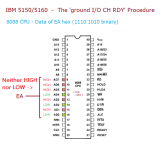
Replaced U18, carefully resoldered the snipped legs, now we have the correct address on the bus for Step 4.1 of the 'ground I/O CH RDY' Procedure.

I continued down the procedure. All good until step 9.1, observing data at the CPU. When I attempt to measure AD0-AD7 on the 8088, the signals are neither high nor low, the logic probe is silent. Other pins give me readings.

1705883663028.png
 
I continued down the procedure. All good until step 9.1, observing data at the CPU. When I attempt to measure AD0-AD7 on the 8088, the signals are neither high nor low, the logic probe is silent. Other pins give me readings.
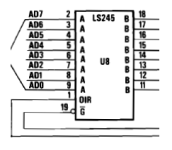
So, step 8 passed, where the EA from the ROM gets as far as the data bus. Per [here], the EA is not getting through U8 to the 8088.

Faulty U8, or faulty control input to U8.

I do not have ready access to my motherboards presently, but looking at the circuit, we expect:
* U8-19 to be LOW, enabling U8.
* U8-1 to be LOW, setting the direction as B-->A

1705885154162.png
 
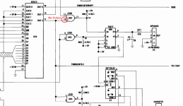
Took at look at U84. On a working board pins 1,2 & 13 should all be HIGH. On our board 1 & 2 are LOW. Those are pull-ups, so i'm assuming failed U84.
 
I may be getting a bit cavalier snipping legs, but they are very easy to fix.

I found out that U2-16 is taking U84-1&2 LOW, but I may have not looked at the 8259A datasheet close enough, because I just realized it's both an input and output pin! Ok, now i'm unsure if the U2 is pulling the line low intentionally or
unintentionally. Originally I just assumed that U2-16 was an input.
 
I compared the U2 signals on the working board vs this board. The only difference is the CAS 0 (12), CAS 1 (13) and CAS 2 (15) pins. On the working board they're all LOW, on this board they're neither HIGH nor LOW.

p.s. ok just checked schematic, I see those pins aren't connected.
 
I found out that U2-16 is taking U84-1&2 LOW, but I may have not looked at the 8259A datasheet close enough, because I just realized it's both an input and output pin! Ok, now i'm unsure if the U2 is pulling the line low intentionally or
unintentionally. Originally I just assumed that U2-16 was an input.
Looking at the circuit, the BIOS listing, and the 8259A datasheet:
Intended for 8259A to run in buffered mode, and the BIOS listing shows that the POST puts the 8259A into that mode.
So 8259A pin 16 will be an output, normally high.
When the 8259A goes to put data onto the AD lines, the 8259A takes its pin 16 to LOW to disable U8.

In the 'ground I/O CH RDY' procedure, the POST doesn't get to run (i.e. 8259A is not explicitly set [via code] to buffered mode). I was hoping to read somewhere in the 8259A's data sheet that upon receiving +5V, pin 16 defaults to an output, driven HIGH, but I could not find that anywhere in the datasheet. An experiment would be to find a spare 8259A, connect up +5V, and see what state pin 16 is in.
 
An experiment would be to find a spare 8259A, connect up +5V, and see what state pin 16 is in.
Agreed, I pulled the one from the donor board and put it in this board, socketed of course, so I can try that tomorrow.

The new (old) 8259A is working, U2-16 is high, and I can see the data on the 8088 now. Still no sign of life with RDR so I'll continue from step 10 and see what else I can find.
 
The new (old) 8259A is working, U2-16 is high, and I can see the data on the 8088 now. Still no sign of life with RDR so I'll continue from step 10 and see what else I can find.
Does a visual of the motherboard reveal where the lightning bolt struck it? :)
 
Does a visual of the motherboard reveal where the lightning bolt struck it?
:ROFLMAO: I know right!?

Ok I spoke too soon. Forgot to try the LPT. To my amazement I can see RDR stepping through it's phases, but no video! I thought maybe something changed with the bench setup, but when I try a working board with the same monitor & MDA card I get video.

p.s. there's no tell-tale beep from RDR either
 
Back
Top