• Please review our updated Terms and Rules here

Help Identifying IBM card from late 1970s

voidstar78

Veteran Member
Joined
May 25, 2021
Messages
707
Location
Texas
While this card LOOKS like it should be for an IBM 5100 or IBM 5110 (c. 1975-1978), I don't think it is. (and physically the card would fit into any slot of those systems)

It's possible maybe the IBM 5120 (aka IBM 5110-3) had a card like this - but I don't think so. The reason I don't think so is because the plastic "sleeve" that the card was in was quite different and wouldn't fit in the normal chassis of those systems.

So what other c. 1970s IBM systems used cards like this? I think the Datamaster/23 used more "ISA" 8-bit looking cards.

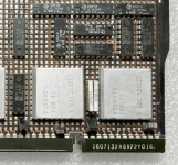
Listed below are the markings of the "siver tin can" chips. If these are consistent with the similar looking "IBM 14" and "IBM 22" chips that are found in the IBM 5100's, then these should be 6KB ROMs - except that nobody knows the pinout of these chips, or how to extract or image whatever 6KB content they might contain.

Note this particular card has no ICs, just some (what I think are) resistor packs (then little black capacitor parts along the four 24-pin green connectors at the "bottom"/base)

2411756 IBM 22 2 1 8135 7290
2729414 IBM 14 9 1 146 266112
2729423 IBM 14 9 1 149 778912
2398577 IBM 22 1 8135 2101 (**)
2729421 IBM 14 9 1 144 216112
2398577 IBM 22 2 1 8148 5001 (*)
2411754 IBM 22 1 1 8134 1705
2729422 IBM 14 9 1 146 991512
2398577 IBM 22 1 1 8135 2101 (*)
2411757 IBM 22 2 1 8143 5230
2411755 IBM 22 1 1 8143 3425

(* same numbers)
(** first number is same as the other *, but stuff after IBM 22 1 differs)

And it's hard to see, but these are "9x9" grid of pins on the backside - but only the outer square and "inner diamond" set of pins seem to actually be used.


1682291316399.png


1682291398464.png

1682291521993.png

@stepleton
 
Last edited:
Those silver cans on the card are all ICs. That was a pretty standard 'backplane' used by a lot of IBM equipment. It could be from a mainframe, S/36 or S/38 era computers, or even internal IBM equipment. I worked on an IBM internal factory-floor communications box that hooked up to a S/370 channel and talked to test computers on the manufacturing floors that used that same backplane. That was my first project at IBM, started in 1979.
 
Well, it's kind of a debate on whether these "silver cans" are categorized as "MOSFETs" or not (that is, the contents inside).

Most of the IBM 5100 and IBM 5110 boards I have, they are mixture of both these "silver can" ICs and the "normal" black ICs.

Here's the only reference I can find to what the inside of these "silver cans" might look like (I think this was from an old Datamation article):

image-57.png


6144 * 8 bits = 49152 (i.e. "48K bits")
Hence why we think they are effectively "6KB ROMs" (and because the ROS modules are CRC'd in 6KB sets-- that is, the CRC is at the end of each 6KB segment).

These silver cans are more like 1" (slightly under), so the "0.23 inch" item above are what should be inside.

For comparison, images of my IBM 5100 cards are here:

Or as a sample, this from SLOT H2 of the IBM 5100 for comparison: (they have a mixture of "IBM 14" and "IBM 22" cans)...
1682317711825.png
The long number of the green plug at the bottom right doesn't mean a whole lot (those plugs come off easily, so they can easily be interchanged with other cards).


But in case it does matter, I just noticed on the backside of this "unknown card":
2411851A2220VCC
1682318123609.png
 

Attachments

  • 1682317632861.png
    1682317632861.png
    358.2 KB · Views: 9
It's been a couple of years and no one can identify this card - so, I'm thinking of sacrificing it, to get a modern high resolution image of what's inside.

That is, there are two proposed approaches: destructive and non-destructive.

The destructive is de-lidding and literally cutting the top off of one of these "silver cans". It'll probably be suspended in some kind of resin therein, and so getting to the actual component is probably going to be destructive. Or in any case, any dust that gets in there may ruin it.

And non-destructive is possibly a kind of kind of x-ray (still learning about the option).


There are enough chips here to maybe try both.
 
Last edited:
Might any IBM cabinet 9-track tape units use something like this? I recall reading the manual of one of those once, and it started talking about the instruction set of the tape system (which at the time, seemed somewhat similar to PALM to me). Can't remember the model - some early 70s/late 60s.
 
In case it helps, there is the "sleeve" or "jacket" that the card was in.

There are two large clips on the top (which is an aspect that the IBM 5100/5110/5120 don't use, afaik in all the ones I've seen). The clip on the top right I think is broken on the end (it should look like the one on the top left, where it can be pressed fully pressed and snap into place -- I imagine to secure the card along a rail/rod).

1682355677305.png
 

Attachments

  • 1682355585596.png
    1682355585596.png
    772 KB · Views: 0
I'd call the "cans" "integrated-ish circuits". Basically a hybrid construction on a ceramic substrate. You can see them on all sorts of IBM gear of the period. For example, the 5150 floppy controller:
555px-IBM_PC_Original_5.25_Diskette_Drive_Adapter.jpg

Given their prevalence in IBM designs, it's hard to say what this particular card belonged to, unless someone recognizes it.
 
Nice find, the FDC on my 5150 doesn’t have that in the corner but it’s an ‘84 system. The other 3/4th of the card looks fairly the same and identical edge connectors.

 
In case it helps, there is the "sleeve" or "jacket" that the card was in.

There are two large clips on the top (which is an aspect that the IBM 5100/5110/5120 don't use, afaik in all the ones I've seen). The clip on the top right I think is broken on the end (it should look like the one on the top left, where it can be pressed fully pressed and snap into place -- I imagine to secure the card along a rail/rod).

View attachment 1256012


that is the style used in 3270 products, like the 3274 coaxial terminal controllers

Also, for the person who scrapped System 34 and 36 boards, don't ...
there is an active community of people trying to restore them
 
Those cans were the packaging used by IBM in that timeframe for the ICs they produced. I used to have one I ripped open that had the IBM microprocessor that we used on my first project, there was no epoxy under the lid, just a chip mounted on the substrate. I may have to look to see if I still have it boxed up. Speaking of 3270 products I think the terminals themselves even used a cage with that style of cards mounted in it for the display and communication logic. They were so common across many products unless someone recognizes it or the part number it could be from almost anything.
 
The 3274s look like they used a similar plastic cage (search for '3274 cluster card' on eBay for some photos) so that isn't a bad guess for sure. I don't see any out there that have the backplane connectors on both the front and back of the card like yours have though. I still remember the lettering/numbering notation for those backplanes which would show up on the circuit diagrams for the machine.
B D
G J
M P
S U
The acronym to remember them was Buy General Motors Stock, Dow Jones Pushes Up (so much for that advice... ;).
 
@modem7 Thanks for that link! But - I'm still confused on SLT vs MOSFET. Is there a difference?

And also from that link, the following quote made me nervous: "In 1968, IBM's widely used SLT modules achieved a reliability rate one thousand times greater than its vacuum tube predecessors." That's great! Except - vacuum tubes weren't all that reliable to begin with, so these SLT modules might not last too long either?


Below are two cards from my IBM 5100 for comparison. The larger "silver-can" on the left is the 9x9 pad variety, then on the right is the smaller 4x4 pad variety (referring to the pin pads on the board itself). The smaller ones here are RWS (RAM), and the link you mentioned has several examples of those (where you can see the 4x4 pins).

The more silver one on the bottom right ("IBM 52") I think is something different - not too concerned about that one.

I tried to get both these images to the same scale as best I could - but for size comparison, the black ICs are the typical 14-pin variety.

1682395938854.png


Are these both (item B and D) SLT technology? The article also mentions IBM SLD, ASLT, MST. How does any of that related to MOSFET? (I'm only mentioning MOSFET because of the old Datamation article that mentioned it).

A = "IBM 52 2395274" (one per each 8KB block), not too interested in

B = "IBM 14 5123129" (I don't know exactly how much each one stores; IBM has the 8-data + 1 bit for parity, there are 21 of these per 8KB RWS board)

C = is this round fan a kind of heat sink? I had another RWS/RAM card where these were anodized red (think IBM was just having fun on that!)

D = not sure if this "IBM 14" is a larger version as what is pointed to "B" (or just coincidence to have the same number there)? Most of these larger 9x9 ones are marked "IBM 22" or "IBM 14". Many of these are on the ROS card and the "disk sort" feature card, so I had always assumed these are all "6KB ROM" chips (that in the IBM 5100, hold the Executive ROS and BASIC and APL set of software). But a bunch of these same sized large 9x9 cans are also on the processor card, which has microcode that (I think) implements the various opcodes of the system - and I just noticed on my 5100 processor card, they are all marked "IBM 22". Maybe 22's are logic stuff and 14's are data storage of some sort?

The "mystery card" has a combination of both 9x9 can IBM 14's and IBM 22's. I just want to do a micro-cut on the top and peek inside. Unless ya'll think this larger "D" can is basically going to look the same as what's in the smaller "B" can?

And I know it's fairly standard to copy a ROM content - would be nice to decode and learn how to copy the ROS content of one if these 6KB chips.
 
@modem7 Thanks for that link! But - I'm still confused on SLT vs MOSFET. Is there a difference?
"SLT used silicon planar glass-encapsulated transistors and diodes. SLT uses dual diode chips and individual transistor chips each approximately 0.025 inches (0.64 mm) square." -- https://en.wikipedia.org/wiki/Solid_Logic_Technology

More details: https://ieeexplore.ieee.org/document/5389188

SLT is a packaging technology, not a transistor fabrication type. As it happens, those were silicon transistors ... not (MOS) FETs, which came along much later.
 
Back
Top