tom.storey
Experienced Member
Hi all,
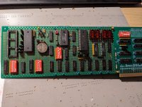
Ive made my own memory expansion for an XT that brings it up to 640KB and gives me a further 128KB to play with as upper memory blocks. The memory expansion seems to work fine, and I can run the machine from it all day without any issues, including with the upper memory blocks.
But it seems that I am unable to boot from floppy disks when I have my memory expansion installed. The machine otherwise runs fine with the memory expansion present. I can boot off the XT-IDE adapter, and run all kinds of software all day, CheckIt reports no problems, things like that.
In a recent thread (https://forum.vcfed.org/index.php?t...ve-no-longer-wants-to-read-any-disks.1241676/) I had hit an issue trying to boot from some floppy disks that I had made in the past and initially thought this might have been my drive flaking out, or perhaps the media going bad, but I am now starting to think that this issue was also caused by this memory expansion problem.
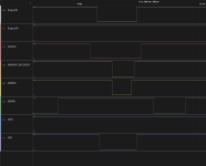
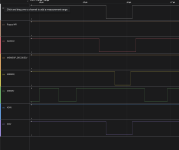
The biggest issue at the moment is when I try to boot a DOS 5.0 floppy disk, the floppy drive goes into some kind of machine gun mode where it has obviously hit the end of its travel, but it keeps trying to go further. Im worried that if this continues it will damage the drive. Once booted from the XT-IDE adapter that I have installed in the machine, I can access the floppy disks just fine and there are no issues, so it seems like it is something related to the early stages of booting from a floppy disk.
Does anyone have any ideas what I should start to look at to figure out why this is happening? I have an oscilloscope and logic analyser if there are specific signals that I should monitor.
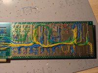
Attached is a copy of the schematic of the memory expansion. The data bus is buffered on to and off of the board via a 74HCT245 that is part of the prototype board that I have created. The direction of that buffer is controlled by the MEMR/ signal, and the tri-state outputs are controlled by the MEMEXP_DECODED/ signal. Most other signals used on the board are also buffered by some 74HCT245's whos direction and tri-state are completely static.
I have an original memory expansion board that came with the computer, and when this is installed it boots just fine from the floppy, so Im wondering what I have done wrong.
Thanks all!
Ive made my own memory expansion for an XT that brings it up to 640KB and gives me a further 128KB to play with as upper memory blocks. The memory expansion seems to work fine, and I can run the machine from it all day without any issues, including with the upper memory blocks.
But it seems that I am unable to boot from floppy disks when I have my memory expansion installed. The machine otherwise runs fine with the memory expansion present. I can boot off the XT-IDE adapter, and run all kinds of software all day, CheckIt reports no problems, things like that.
In a recent thread (https://forum.vcfed.org/index.php?t...ve-no-longer-wants-to-read-any-disks.1241676/) I had hit an issue trying to boot from some floppy disks that I had made in the past and initially thought this might have been my drive flaking out, or perhaps the media going bad, but I am now starting to think that this issue was also caused by this memory expansion problem.
The biggest issue at the moment is when I try to boot a DOS 5.0 floppy disk, the floppy drive goes into some kind of machine gun mode where it has obviously hit the end of its travel, but it keeps trying to go further. Im worried that if this continues it will damage the drive. Once booted from the XT-IDE adapter that I have installed in the machine, I can access the floppy disks just fine and there are no issues, so it seems like it is something related to the early stages of booting from a floppy disk.
Does anyone have any ideas what I should start to look at to figure out why this is happening? I have an oscilloscope and logic analyser if there are specific signals that I should monitor.
Attached is a copy of the schematic of the memory expansion. The data bus is buffered on to and off of the board via a 74HCT245 that is part of the prototype board that I have created. The direction of that buffer is controlled by the MEMR/ signal, and the tri-state outputs are controlled by the MEMEXP_DECODED/ signal. Most other signals used on the board are also buffered by some 74HCT245's whos direction and tri-state are completely static.
I have an original memory expansion board that came with the computer, and when this is installed it boots just fine from the floppy, so Im wondering what I have done wrong.
Thanks all!
")