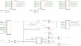
I've devised a schematic that I think provides port 300h, 301h ordering for both reads and writes hence should support fast transfers in both directions. For reads it's exactly per the 'chuck-mod'; but it uses dedicated transceivers for reads and writes, a single byte-buffer and a few other bits.
Here it is (image file).
Theory of Operation
IO-Reads:
1. Port 300h.
- /CS0 asserted, /CS1 not asserted, IDE-A0..2 not asserted
- Buffer-load asserted, buffer-/OE not asserted
IDE devices interprets this as a data transfer:
- IDE D0..7 presented to the ISA bus via the read-transceiver
- IDE D8..15 loaded into the byte-buffer
2. Port 301h.
- /CS0 not asserted, /CS1 asserted, IDE-A0..2 not asserted
- Buffer-load not asserted, buffer-/OE asserted
So the IDE device ignores the cycle, and the byte-buffer presents the previously loaded IDE D8..15 onto the ISA bus as D0..7.
This is exactly the same as the Chuck-mod.
IO-Writes:
1. Port 300h.
- /CS0 not asserted, /CS1 asserted, IDE-A0..2 not asserted
- Buffer-load asserted, buffer-/OE not asserted
Data presented on the ISA bus D0..7 is transferred via the write-transceiver and loaded into the byte buffer (this is the LOW byte of the Word transferred from the CPU).
2. Port 301h.
- /CS0 asserted, /CS1 not asserted, IDE-A0..2 not asserted
- Buffer-load not asserted, buffer-/OE asserted
The IDE device interprets this as a data transfer:
- IDE D8..15 are presented via the write-transceiver to the IDE directly
- IDE D0..7 are presented via the byte-buffer
EDIT - I realised this circuit had no way to write any other port, so have added logic so it won't flip the IDE /CS0 & /CS1 signals except for ports xx0h and xx1h - ISA singals /IOW, A1, A2, A3 all need to be low, or put another way, it will aways trigger a write command unless it's port xx0.
A second pair of eyes on it would be very much appreciated
")
It would need new BIOS code of course. The idea is for CPLD implementation (I'm not proposing a physical circuit).