• Please review our updated Terms and Rules here

I wish to create a new DMA/RAM expansion card for the Tandy 1000 line.

Hah! I guess it pays to double-check your work. I just tracked down and downloaded the 1000 HX service manual because I wanted to see what its memory map looked like (in the name of making sure what I was building I didn't step on the HX's built-in DOS ROMs, just in case) and its clearer diagrams produced a forehead-slapper; I'd assumed that table J12 on page 6 of the EX manual actually reflected the physical layout of the expansion connector. It turns out it has the columns reversed. Aaaargh! :curse:

Better to find that out now than after having some test cards made. But it does mean I have to go back and fix my custom library footprints that took like an hour and a half to make. (not to mention having to reroute the PCB) :roll:

Oh yes, that one will screw you over.

Reminds me of a mistake I made, where I was poking around with a multimeter and accidentally slipped the probe, crossing the +12v with one of the data pins adjacent to it, bricking the board. I was able to narrow down the buffer chip on the motherboard that was responsible, and replace it, so it works again, but if you don't note that the A and B sides are reversed between the PLUS and ISA, you'll likely fry whatever is connected directly to the data bus (another reason for having a '245 buffer, should those two somehow cross).
 
Yeah. I was so shaken from almost committing to the mistaken layout I actually printed out the main board PCB art in the manual and traced out some of the obvious-as-to-function lines like connections to ground to be absolutely sure the orientations are correct now.

Spent a bit of time today finishing a schematic for the CF port and took a shot at combining it with the RAM and clock. Fiddling with the rat's nest for a while has convinced me to stick with my board sandwich plan for memory (and clock) on one board and I/O on the other. Just the IDE port is trivial with ROM already on the other board, so I'm going to see how the serial port from the floppy/serial plans out there fit.

On one hand doing it this way would make the CF port on my I/O board useless to anyone that has a different memory card (or wants CF with 256k), but the serial part could probably be built stand-alone and potentially be useful. For that board I guess I should make at least a token attempt to make sure the clearances around the bus connector would let it fit a normal PLUS card stack.

(I suppose it might be worth doing on the other one? Potentially the ROM/Clock part could work without the RAM chip installed.)
 
Just about finished laying out a combination CF Port/Serial card to piggyback on the RAM/ROM/Calendar board. At this point I think I've figured out just enough about Kicad's PCB layout tools that I I'm going to go back to the RAM/ROM board and tweak it so it includes some things I neglected the first time, like heavier traces for VCC, and then maybe it's go time.

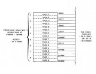
Stepping back a bit, though, I have some questions about how video RAM is mapped in the pre-TX/TL systems that I'm wondering if someone can clarify. The T1k FAQ here and some other articles seem to imply that as RAM is added to a T1000 the base memory location of the video buffer (which is also double-mapped at B800h) moves higher. (The latter article names some specific examples of games that supposedly break because base level of the video buffer moves out of the region in which it would reside in a PCjr.) I'm trying to wrap my head around how that would work based on the sketchy information in the EX and HX tech manuals. It sounds like the buffer *has* to reside inside the built-in 256k RAM, the video circuitry can't just arbitrarily pull pixels from any installed memory, and there's this diagram that shows where the possible RAM pages reside in memory using 00000 as the base:

T1k_VRAM_Pages.jpg

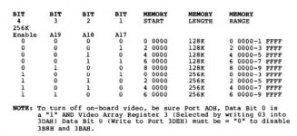
But later in the manual there is this chart which seems to imply that the starting point of the page VRAM is stolen from *does* move upward as RAM is expanded:

T1k_VRAM_Base.jpg

In 128k increments. The manual doesn't seem to explain this literally anywhere (or it's in such sparse language I'm missing it), but does this imply that the addresses on the bus connector are actually being remapped by the video chip with regard to the base RAM area?

Why this matters is if this is what is happening I'm pretty sure the A000h jumper on my RAM card design isn't going to work to give 704k RAM, because I was stupidly assuming that the VRAM was moving the base of memory upwards, not stealing it off the top. If this is how it works it seems that it's always going to steal 16-32k (by default) from just under the 640k barrier, so there will be a hole between there and any RAM I put in the A000h page.

I wonder if I can convince USE!UMB.sys to use it?

(*EDIT*: Actually, now I'm wondering if it might theoretically be possible to put a 512k expansion in an EX/HX and have it behave like a 768k-expanded TX/TL/etc. by manipulating the NMI Mask Register so it uses 8000h for the start address of the remapped base memory with "256k Video RAM" enabled, a combination the tech manual seems to deem illegal. Presumably that would require a BIOS patch?)
 
Last edited:
Well, it certainly does steal the top 16-32K and place them in the UMB section for video and HI RAM. Whether it pulls it physically from the onboard 256k, you might know better than I.
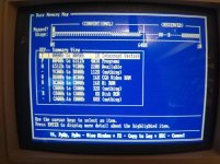
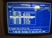
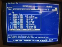
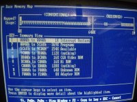
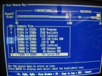
The next few pictures are hasty screen captures from Checkit3. This is my HX, with the Tandy DMA/RAM card installed. C800h-CA00h is my XT-CF card, so that can be safely ignored, but the other blank areas could potentially be mapped as UMB for Lotus 1-2-3 and other programs that might take advantage of it, who knows.

IMG_20190611_180730206.jpg
IMG_20190611_180847668.jpg
IMG_20190611_180756147.jpg
 
Last edited:
Well, it certainly does steal the top 16-32K and place them in the UMB section for video and HI RAM...

Eyuck. I'm pretty sure your screenshots verify that just tacking 64k after the 640k limit and using a device driver that works on a normal XT (There's a "704k" device driver floating around out there on the DOS archives for doing so that I was going to try) to raise the BIOS RAM ceiling isn't going to work because there's going to be an actual memory hole that can't be shoved up to the top. (At least in a 64k increment. I'm itching now to find the 1000 TX tech manual and see if it goes into detail about how the 768k configuration available for that machine worked... I *think* that machine also used the same, or nearly the same, version of the video ASIC?)

The description of how the base RAM is slaved to the video chip in the tech manual essentially confirms that it *must* be some sort of memory address translation. I wish it described it in more detail, however, because... wow. The fact that the manual calls the register that controls how this mapping is performed the "NMI Mask" kind of implies it might not actually be all in hardware? (NMI handlers are infamously used in some oddball PCs to emulate with software missing hardware or paper over incompatibilities.)

But I suppose ultimately the TL;DR is it's likely the only way I can use the A-page RAM is as a UMB. This got me re-thinking the idea of coming up with some harebrained scheme to instead map 128k of the 512k RAM into the D and E pages. Could do it by selectively inverting a couple of the address lines to the RAM when the chip select pointed to those pages, maybe? Ugh.
 
I think most people will be happy just having that extra 384K to bring it up to a more functional 640K, since most programs that needed more than that needed a meg or more (not a whole lot out there that actually used UMB, to my knowledge. That was kinda my idea all along, once I can get back to this project (it's currently a half-finished protoboard with a ratsnest of wire). If you feel brave enough, you could pick up one of Lo-Tech's 1MB RAM cards, connect it to your EX with an ISA-PLUS ribbon adapter, and play around with the settings to see what lights up and if/how the machine can recognize anything past 640K.
 
I just finished skimming through the TX's technical manual, and the takeaway is that you *probably* can't just poke new values into the NMI mask register in an 8088-based T1k to shove the video memory above the 640k mark. It does use the same "Big Blue" video ASIC as the 8088 machines, and the ASIC has RAM slaved to it that can be both VRAM and system RAM when you have a machine with just 640k. The difference seems to be, though, that all the "other" RAM in the system is physically mapped *below* the start of the BB RAM, not above it, so the location of the video page frame is "literally" at the end of main memory instead of a page being flipped/remapped from the bottom?

There *is* still an NMI mask register like the 8088 boxes and there's a table that is a superset of the one in the HX manual though so... heck if I know. I'm kind of curious what would happen if you stuck the value a 768k TX runs with (which limits the Tandy graphics RAM to the B000h window) into an EX/HX with expansion memory; would you end up with a 384k machine with the "Big Blue" essentially acting as a video card only, would it crash hard because that mode needs alternate RAM physically mapped at 0000h... or what.

Someone far, far more competent than I am at 8088 machine language needs to disassemble the boot ROMs and document how the initialization routines decide what to stick in that register.
 
Mulling this over for a while instead of sleeping an alternative theory of how all these machines might work has occurred to me, and it makes me wonder if I need to re-check a base assumption:

I've seen it suggested several times to stick a lo-tech RAM card into an EX/HX with an ISA adapter. Has anyone actually done that? And if you did, how did you set the switches?

I ask because an alternative interpretation of that NMI mask table is that all 1000's move the base location of Big Blue based on installed RAM. And if that's the case, wouldn't a Tandy RAM card need to start counting from 00000h, not 20000h or 40000h (128k original 1000 and EX/HX, respectively)?

If Big Blue moves its base location up in 128k intervals that explains a *lot*. And it also means my RAM card's mapping (based on what you'd do for a 256k XT) is all wrong.

Has anyone made a DIY RAM expansion for these before?

They do work in the EX / HX machines - you do need to disable the 1st 256kb of ram tho. as for the upper ram I'm not sure.
 
They do work in the EX / HX machines - you do need to disable the 1st 256kb of ram tho.

Have you tried this first hand? I've been searching in vain for any posts where someone relates actually plugging one of these cards into a Tandy 1000 of any sort (or at least 1000/A/EX/HX) to use as main RAM, if you have a link to such a post I'd love to see it.

I found the "Service" manual for the original T1k on Archive.org

https://archive.org/details/Tandy_1000_Computer_Service_Manual_1985_Tandy

This manual has much the same information as the "Technical" manuals but it includes a couple "Theory of Operations" sections that fill in some of the blank areas I complained about earlier. And what I'm piecing together is that a RAM card for the 1000 series needs to start at 00000h. Page 40 of the service manual:

The RAM is located at an address determined by the memory configuration control port. In a 128K system that address is normally 00000-1FFFF...

Also, this manual has an account of how the initialization process works starting on page 75, and here's a couple of passages that make it sound like the RAM controlled by the Big Blue is *not* located at the bottom of the memory map when the system is started:

The next step is to initialize memory for the CPU to use as a scratch pad for analytic decisions.
The system/video RAM is moved to begin at address A0000 hex. (A write to memory configuration
port A0 also disables "non-maskable interrupts".)....

A 180h byte area of video/system RAM is tested to be used for "stack" and "data" by the CPU.
The test consists of writing throughout the area in the following order all 0000's, 5555's, AAAA's
and FFFF's from address BBE80 to BBFFF. (All video accesses are through the fixed video address
window B8000— BFFFF)...

(And now the important-sounding part)

After establishing that a portion of the video/system memory is functional, you must determine the
amount, if any, of available external memory. The external memory depends upon the DMA channel
#0 for "refresh" and the DMA depends upon the Counter/Timer counter #1 for the "requests".
Thus the 8253 Counter/Timer is tested. A rotating bit pattern is written/read from counter #2 with
the output gate disabled. If it is faulty, the following message is displayed:

11 FAULTY WRITE AND READ OF 8253 CHANNEL 2 REG' 1

If the test is passed counter #1 is programmed for a pulse at 15 microsecond intervals. Now the
DMA controller is tested in a similar manner to verify its existence and Draper operation. If it passes,
channel #0 is programmed for "refresh" operation and enabled.

Next the external RAM memory size is determined. This is accomplished by reading a word of data
at each 128K boundary complimenting the data, writing the data back, delaying a short time, and
then reading it. When the data is wrong, assume no memory. The search is terminated. The add-on
memory is address mapped to start at 00000 hex and be contiguious in 128K segments up to 512K
total. When the amount of external RAM is determined, the video/system RAM is mapped to reside
on top and be the uppermost 128K.
At this point, the message:

' "MEMORY SIZE = XXX K ' '

appears on the screen. If there is a possible fault, the displayed memory amount is different from
the known amount. If only the base amount of 128K is accounted for, the most probable fault is
an inoperative DMA refresh. Other amounts less than the full amount indicates a faulty memory."

(The wording of this section kind of freaks me out a little because a possible interpretation of it is that the Tandy won't do the memory test if it doesn't detect DMA, but I think there's evidence like that weird undocumented SRAM expansion for an original 1k that was ebay that that isn't the case.)

I'll grant that the word "map" in there is open to interpretation, but... I also looked in the Tandy 1000 *technical* manual that's linked at the beginning of this thread, and while it doesn't have the startup theory of operations section it does have section explaining the operation of the RAM card starting on page 73, and it explicitly says that the base address of the first RAM card is 00000h.

I'm starting to think the only way to definitively answer this is to breadboard a RAM card with the start address switchable between 00000h and 40000h.
 
Have you tried this first hand? I've been searching in vain for any posts where someone relates actually plugging one of these cards into a Tandy 1000 of any sort (or at least 1000/A/EX/HX) to use as main RAM, if you have a link to such a post I'd love to see it.

No but many of my customers have - it's quite easy to turn off the 1st 256kb of ram on the 1 MB board.
 
No but many of my customers have - it's quite easy to turn off the 1st 256kb of ram on the 1 MB board.

I'm sure it is. What I'm not convinced of at this point is whether that's the correct setting for a RAM card used in a Tandy 1000, which is why I'd like first-hand confirmation from anyone who has the experience as to what physical mapping they used for adding memory to an early T1k with a non-Tandy expansion board. (The decoding scheme I came up with for the board I'm working on was essentially the same as a Lo-Tech with the switches set to work in a 256k 5150 or whatnot, which is how you're advising people to set the board.)

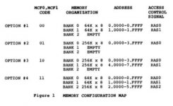
More digging, this time in the Tandy 1000 HX technical manual, turned up this table in the section talking about the proprietary chips they use on the Plus card:

Screen Shot 2019-06-12 at 2.35.05 PM.jpg

Note the "ADDRESS" column: In all configurations Bank 0 starts at 0.0000h, not 4.0000h, the latter being where you'd expect RAM to start if you were backfilling a normal XT with 256k on the motherboard. This jives with the operational description in the original T1000 manuals. And if this is right, to use a lo-tech RAM card in the machine you'd want to set the switches to enable 384k (or possibly 512k, there are hints that a 768k mode may well be available. Does anyone actually have the apparently-rarer 512k version of the Plus board in their EX or HX? I'd love to see Check-It output from that) starting at 0h and the Tandy would then map the built-in 256k starting at 60000h, producing a 640k-minus-16-or-32k configuration.

If it's actually working for people who've set the switches to start at 256k then the word "map" in this gets more interesting:

Next the external RAM memory size is determined. This is accomplished by reading a word of data
at each 128K boundary complimenting the data, writing the data back, delaying a short time, and
then reading it. When the data is wrong, assume no memory. The search is terminated. The add-on
memory is address mapped to start at 00000 hex
and be contiguious in 128K segments up to 512K
total. When the amount of external RAM is determined, the video/system RAM is mapped to reside
on top and be the uppermost 128K.

Can the Tandy shuffle RAM it finds at 40000h down to 00000h, IE, can it detect non-contiguous RAM on 128k boundaries and compact it? That seems to ride on the interpretation of "The search is terminated." Does it terminate when it has its first failure to find RAM, or does it mean the search terminates and moves on when it's done walking through all the 128k segments under 640k? It makes more intuitive sense that it can "only" move the Big Blue chip and the RAM slaved to it around.

I have a few RAM chips coming on a slow boat from China; I wanted to skip this step but maybe it's the better part of valor to try sticking one on a breadboard and connecting it to the Plus connector with a jumper harness to see what works. That's going to be nasty.
 
Last edited:
Yes, those RAM chips for the Tandy RAM card are a bitch to track down. I did manage to find some, so I have spares if mine ever go. The ASIC in the center of the board though is another story. If that ever goes, the card's hooped unless you can track one down on eBay.

I know at least that LGR upgraded his Tandy 1000 with that Lo-Tech card. https://youtu.be/malgCK7qHQA?t=531
It has dip switches for each 64K page, so you'd be flipping them in pairs.

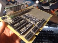
I was hoping to do what you're suggesting, only on a perfboard, rather than a breadboard, and this was to be my first prototype for this project so I could narrow down exactly which RAM pages were usable, and widdle it down to about half the component count.
IMG_20190612_165800600.jpg
I went to plug it in and make sure that nothing was crossed.... And something was crossed that prevented the machine from POSTing. This is where I left off.
Knowing that the T1k searches for 128K pages helps, and it kinda sucks that you gotta flip through each manual in the series in order to figure out the commonalities.
 
I know at least that LGR upgraded his Tandy 1000 with that Lo-Tech card. https://youtu.be/malgCK7qHQA?t=531
It has dip switches for each 64K page, so you'd be flipping them in pairs.

That video may have just proven immensely useful! It's high-res enough that you can see what he set the switches for, and it looks like he has all switches up on SW1 and the first two up on SW2. According to the chart on the back of the board that means he's actually got it set to provide RAM for the entirety of the 640k address space, and the machine apparently will POST like that.

640k + the built-in 128k is actually the memory mapping used by the Tandy 1000TX, so unless his Lo-Tech card is sitting on top of the built-in RAM at 8000h (which is a possibility, that kind of clash might actually be something you'd get away with) this *may* demonstrate that even the old Tandy BIOSes can grok that and program the mapping of Big Blue appropriately. It is frustrating because per this:

Knowing that the T1k searches for 128K pages helps, and it kinda sucks that you gotta flip through each manual in the series in order to figure out the commonalities.

It really is a pain in the rear, because different versions of the same chart explaining the Big Blue memory mapping register appear in every manual, but none of them explain it entirely; they seem to have decided that only the settings that applied to each model *when it was introduced* are relevant, it doesn't explain every different possibility the chip can handle.

(This is why I'd love to see the Check-IT output from an EX or HX equipped with the 512k Plus board, because there are unresolved possibilities for what happens if you have expansion RAM to 7FFFF in a system with a 256k Big Blue.)

How hard would it be to dumb down your test board so you just have one 512k RAM mapped from 0h to 7FFFF? The decoding for that should be really trivial; this is a terrible idea, but in principle couldn't you just connect A0-18 straight across, use A19 as your chip enable, and essentially dispense with decoding entirely? (A19 will be low whenever the machine is in the bottom 512k, and of course MEMR and MEMW will need to be active to make the chip read or write, so... bang, no decoders needed? I feel like this is wrong but I can't quite pin down why.) I have three theories what you'll get out of this:

A: 640k! (Plus possibly some RAM sitting in the A0000 page) This from Big Blue mapping its 256k from 8000-BFFFF. This would be optimal.

B: 512k, because the Tandy won't do a 256K Big Blue at 80000h and instead exiles Big Blue to B0000 like in a fully expanded TX. (Which means you'd need to either add another 128k to get the backfill, or pull back to 384k so it'll map Big Blue to its documented 60000h position and keep double-mapping the last 32k)

C: Something less useful, but probably not something that will smoke the computer.
 
Last edited:
It assumes that the shot of him putting the card in is actually the configuration that allowed him to boot, but yes, that seems to be the implication.

How hard would it be to dumb down your test board so you just have one 512k RAM mapped from 0h to 7FFFF? The decoding for that should be really trivial; this is a terrible idea, but in principle couldn't you just connect A0-18 straight across, use A19 as your chip enable, and essentially dispense with decoding entirely? (A19 will be low whenever the machine is in the bottom 512k, and of course MEMR and MEMW will need to be active to make the chip read or write, so... bang, no decoders needed? I feel like this is wrong but I can't quite pin down why.)
Well, the board is all wired up already, it just doesn't work atm. I've got the parts on hand to breadboard it separately. Could give that a shot when I get the chance (won't be tonight) and see what happens.

Well, if it lets the magic smoke out, I happen to have a spare motherboard for my HX that I picked up as a result of a dumb mishap on my part that involves a multimeter, non-sharp probes, slippage, and a +12v pin that smoked a buffer IC that I was finally able to track down, but I'd rather avoid that outcome, since I just fixed the thing a few months ago :/

The outcome isn't too much of a worry so long as you don't get the +12v or -12v crossed with anything, since everything else is 5v logic.
 
Assuming the new theory about how the T1000's initialization system actually works is correct I think the worst thing that could possibly happen is bus contention from having the RAM on the expansion bus overlapping with Big Blue because it turns out, say, that the EX/HX simply stop counting external RAM if they find RAM up through the 384k mark, assumes 6000h is going to be open, and places the Big Blue there instead of 8000h.

(That's the thing, those annoying tables in the tech manuals don't show a "truth table" for a 256k Big Blue at 8000h, but it could just be because it reflects a setting they didn't have hardware for at the time.)

The thing that bugs me a little is the question of if you'd necessarily see bus contention if it happened. For instance, Re: the LGR video, the original T1000 manual only shows the mapping register settings for putting the starting address for the Big Blue up to the 512k mark. The 1000 TX manual *does* show a setting for 640k. (IE, that's the condition in which it *just* uses the Big Blue memory for VRAM in the B-page.) So my question is, assuming those switch settings are actually what LGR is using, is the older T1000 also setting up Big Blue the way a 1000TX would, or is it possible he's got the last 128k of the RAM on the lo-tech doubled on top of Big Blue, and the system just doesn't care because the contents of the two RAM banks are successfully staying in sync.
 
the system just doesn't care because the contents of the two RAM banks are successfully staying in sync.
Possible in theory, so long as nothing sneezes. To be safe, I'd have a switch to lift the first 256K on that PLUS board, so if your original RAM is working, you don't have any hickups. And then the other question, if it is able to overlap, is there anything that will complain if it doesn't find that onboard RAM, but the card is fully populated.

Yeah, basically, one of us is going to have to slap something together to find out how it will behave, and then proceed from there.

I'll see if I have time on the weekend to kludge something together.
 
If you don't beat me to it I'll take a shot at it when my RAM chips arrive. I picked ePacket delivery so... latency is a bit of an unknown.

I do want to see what happens if you do skip the first 256k. My tentative breadboard plan is a 74LS138 to divide the bottom 512k into four parts and a 74LS08 to combine various combinations of 128k pages.

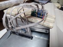
Well, I rigged up a PLUS to breadboard lead pack, hooked up a 512K chip as you suggested....
IMG_20190614_001802405.jpg
And it works!
It even passed an extended memory test.
IMG_20190614_005038668.jpg

Looks like this project could end up retardily simple if it didn't show 640K RAM instead of 512K or 720K, because this raises questions as to why.
IMG_20190614_001818152.jpg
IMG_20190614_001831318.jpg

Now, is the onboard RAM is being pushed to start at 7FFFFh, while the expansion RAM starts at 00000h, and then just cuts off any extra that spills over that 640K limit? Will it behave differently if slap on address decoding and start the expansion RAM at 40000h? I don't think that UMB is going to be an option for this machine, but this is more than enough to churn out a functional RAM expansion board, with plenty of room for other goodies.

While this appears to be functional, and a hell of a lot easier than we were imagining it should be, I'd still stick it behind a '245 buffer, as a matter of course, if you're going to actually use it this way.
 
Hah! So, yeah, that's definitely a data point.

The head scratcher that's remaining here for me is why Check-It is still showing a video page being swiped from the end of conventional RAM. I wish it was possible to read the memory mapping register for the big blue. (Tech manual says it's write only.) One of two things must be happening at this point:

A: Big Blue is getting mapped to the 512k mark, but when running in that mode BB still grabs a page from the end of RAM and masks out the A-page. (Perhaps detecting 512k base memory makes it disable half its own memory, so it becomes the same as an original T1k?)

B: It put BB at 384k, so technically the RAM is conflicting right now but it's not bothering anything.

How to figure that out...
 
Back
Top