• Please review our updated Terms and Rules here

I wish to create a new DMA/RAM expansion card for the Tandy 1000 line.

I'm game to try. With the LS151 reconnected I can deselect the 384-512k bank from the SRAM... although it seemed the 151 introduced some timing errors that caused other issues. But I could disable that bank while the system was running and if it continues to just magically work that would be telling.

Hmm had you scoped the OE pins on the motherboard DRAM while running a RAM check on the 384-512k pages? (Which SRAM was also in that space.) That should be quite telling and tell us right away if both RAM chips are driving the bus.

Edit: Another thought -- would just removing the extra 128k of RAM turn the EX/HX into a 128k system? I wonder if it works that way. I'm curious now too! That might be the way to go if we find there is a BUS conflict... Easier if someone wants to use a single chip SRAM board without deselecting. I will test this out tonight .. my EX has zero RF shields anymore (is anyone surprised?!?) so it's easy to yank RAM chips.
 
Last edited:
Tandy 1000EX address lines:

dySJqA0.png


Tandy 10000HX address lines:

kmWgG96.png


Look basically the same. So why all those pulses?
 
Now I need to check and see if you can do that in BASIC... ;)

Oh, foo. At least the version of BASICA included on the EX disks doesn't let you allocate more than 128k to graphics pages, I get an "Illegal Function Call". I guess color me not surprised they didn't bother updating that for the 256k Big Blues. (Unless the binary on the HX dos disk is different.)
 
Yeah hi! I just have been so busy haven't had time to read here much. And yeah I wondered how you even got those connectors in the first place! I just made my connector out of a random 40 pin header and a single strip of 11 more pins ..... It's janky but it seems to work fine. Just need to make sure you align it correctly before you push it onto the connector. Ideally we would want to make a board with the SRAM, a ROM and the 8-bit CF support all on one. Way above my abilities LOL!

Yeah I know the feeling! I've had no time in the past month to do any retro design work at all. :(

I was buying the 64 pin R/A connectors from Digikey and cutting them down with a micro-saw - thankfully the results where quite good.

Agreed, RAM + CF-IDE + DS1315 Clock was what I'd been working on but I've not had time to finish the electrical design, let alone get some PCB's made up. I was mashing the Lo-tech 1MB design together with a simplified CF-IDE design and the DS1315 hooking into the IDE ROM socket.
 
Hmm had you scoped the OE pins on the motherboard DRAM while running a RAM check on the 384-512k pages? (Which SRAM was also in that space.) That should be quite telling and tell us right away if both RAM chips are driving the bus.

If one of the two banks is actually quiescent while the other one is serving video RAM accesses that might do it. The gnawing concern I might have is if when adding a second bank of DRAM to Big Blue someone may have thought it'd be a good idea to add interleaving to the mix, in which case both banks would always be heartbeating, always... but I suppose worse case that would just give you a false positive, not a false negative.

The HCT373 latch chips may be the issue but I need to check as A12-A15 are not multiplexed so just go through a HCT244. Need to check for the spikes there. OE on that 244 is still driven from AEN which comes from the light blue via HCT244 .... but yeah something is very odd and the spikes are likely causing my issues on my HX as the SRAM will be pulsing the databus when it shouldn't be. (If A19 pulses low for 40ns while MEMR is also low)

So these 40ns pulses are constant, and actually going on why MEMR/MEMW are active? That would be severely broken behavior. Some instability in the address lines early in the bus cycle might be okay, there's a timing chart in the manual that I think can shed some light on how long would be okay, but if they're not stable outside of that window I'm perplexed how the machine is working at all. Big Blue is also on the other side of those address latches, I'd think it'd get ticked off at the address lines changing during MEMR/MEMW too.

I'm game to try. With the LS151 reconnected I can deselect the 384-512k bank from the SRAM... although it seemed the 151 introduced some timing errors that caused other issues. But I could disable that bank while the system was running and if it continues to just magically work that would be telling.

That *might* just be messy wiring. I know Blackepyon was saying in a thread about his CF board that he was getting inscrutable errors because of the distance he had between the '245 buffer on his point-to-point card and the bus connector.
 
If one of the two banks is actually quiescent while the other one is serving video RAM accesses that might do it. The gnawing concern I might have is if when adding a second bank of DRAM to Big Blue someone may have thought it'd be a good idea to add interleaving to the mix, in which case both banks would always be heartbeating, always... but I suppose worse case that would just give you a false positive, not a false negative.

Heh that's possible too! So many possibilities! I'll post back what I find.

[/QUOTE]So these 40ns pulses are constant, and actually going on why MEMR/MEMW are active? That would be severely broken behavior. Some instability in the address lines early in the bus cycle might be okay, there's a timing chart in the manual that I think can shed some light on how long would be okay, but if they're not stable outside of that window I'm perplexed how the machine is working at all. Big Blue is also on the other side of those address latches, I'd think it'd get ticked off at the address lines changing during MEMR/MEMW too.
[/QUOTE]

Not quite constant, but lots of them. Talking to a friend about it, his theory is they are so short at 40ns that a lot of older slow stuff like the DRAM (and I assume Big blue) just won't care or do anything with pulses that short. I haven't put the logic analyzer on it yet to see if all the stars align but the fact I see those short pulses on the data bus is very suspect. I need to check the bata bus with the 55ns SRAM removed .... I ran out of time yesterday to troubleshoot more.

That *might* just be messy wiring. I know Blackepyon was saying in a thread about his CF board that he was getting inscrutable errors because of the distance he had between the '245 buffer on his point-to-point card and the bus connector.[/QUOTE]

I totally believe that my crap wiring might be leading to issues..... also the LS151 I have (only one) is old and slow since it's not a F/ACT/HCT part. How crazy that Blackepyon had such issues .... could likely be what my problem too when I tried to wire in the 151. I just would have never thought things were so sensitive considering the drivers on the motherboard side but hell I'm the furthest from someone who knows what they are talking about!
 
So, because just can't leave well enough alone, I've been fiddling around in BASIC and I think I've learned some interesting things. The first is, yes, unfortunately you can't read that register at port &hA0. But you sure can cause some havoc by writing to it.

Referencing the Tandy 1000 TX tech manual, page 44, I tried putting in various values. It looks like doing this:

out &ha0, 152

does no damage to my system, because that appears to be the right value for a system with a 256k Big Blue and 384k of base RAM. Next thing I tried was this:

out &ha0, 158

That's the value for that hypothetical Tandy 1000 TX with 640k and a 256k Big Blue. (Which never existed.) The machine crashes if I exit BASIC, it apparently can't load command.com (brutally ripping out a chunk of RAM without changing the top of RAM register is no doubt to blame), but it doesn't crash BASIC immediately so I tried this:

def seg=&h6000
print peek(0)
result is 7, which seems to be what the unoccupied spaces in the memory map return for my 1000 EX
poke 0,(some number other than 7)
print peek(0)
result is still 7

So I've apparently succeeded in switching the Big Blue RAM upwards. I tried changing the def seg to &h8000, and it's also empty, so it appears I've actually managed to configure an EX like a TX. So the hardware is capable! (Now I'm pondering the possibility of a custom ROM...) So... Then I tried this:

out &ha0, 150

This is the command that should drop Big Blue down to the 256k mark. THIS SHOULD BE A CONFLICTING CONFIGURATION, but the machine doesn't crash. If I repeat the DEF SEG test at 60000h I can now read and write memory, so RAM is back at the 384k mark, but if I DEF SEG at &h8000 I can verify that RAM is ending at 512k mark.

Honestly this seems like a pretty definitive test that having the SRAM on top of Big Blue doesn't crash it.
 
Last edited:
... addendum to last post. I just tried this:

out &ha0, 148

Which is the value for a 256k Big Blue with 128k of RAM expansion; that should nest Big Blue's RAM entirely on top of my RAM expansion. And if I do this:

def seg=&h5c00
poke 0,65

The character in the uppermost right corner of the screen turns into an uppercase A. So QED, the SRAM and Big Blue can sit on top of each other without melting.
 
WOW, that's fascinating. I guess they are both driving the bus at the same time and since they are conflicting it is just "OK." I'm not sure how good this is for the respective chips though!

So theoretically we can configure it to be 512k + 128k which would get rid of the double-driving the data bus as well? (And not crash anything) as it should just stop both driving that top 128k..... Hmmm. Crazy it can be configured on-the-fly like that.

And 640k + 256k -- neat! What would that give us exactly? I wonder if big blue would put that 256 into the upper address space in a way that was usable somehow?
 
Sorry, I am late to the conversation, so I may be dipping into something that's already been covered, but...

I was talking to a guy on Youtube about this very thing.

I'm wondering how the non-DMA system refreshes the 256k onboard RAM. On the PC and XT, DMA 0 is used to trigger dram refresh.

My supposition is that the non-DMA Tandies may be using the video circuitry for dram refresh, kinda like the apple 2 does? The ram is rated twice as fast as the system clock, and the video circuitry accesses it with an offset clock so it doesn't screw with the CPU's bus cycle (according to my understanding, that is; I am pretty dumb though!). So since the video circuitry has to read the video ram anyway, it might as well just read/refresh the rest of it during vblank anyway.

I am also recalling reading somewhere (I can't remember where, and I can't find it again, so again I may be full of poo), that the Tandy always maps onboard ram as video memory, never expansion card memory. This makes me wonder if there's some extra special sauce going on with the onboard RAM that, if it were removed and all system ram put on an SRAM card, would cause the video circuitry to stop working.

This also brings up the question of whether a DMA board even needs to have any RAM on it at all. If we just want DMA for running a sound blaster, then we can just use a lo-tech sram card for the memory (since it doesn't need refresh), and the internal 256k DRAM will still get refreshed (maybe) by the video circuit (assuming I am not full of poo).
 
Last edited:
WOW, that's fascinating. I guess they are both driving the bus at the same time and since they are conflicting it is just "OK." I'm not sure how good this is for the respective chips though!

Yeah, I'm not comfortable leaving it like that forever, which is why I'm being nitpicky about making *absolutely* sure there's not a conflict before we say that a no-decoding 512k base RAM solution is OK. ;)

So theoretically we can configure it to be 512k + 128k which would get rid of the double-driving the data bus as well? (And not crash anything) as it should just stop both driving that top 128k..... Hmmm. Crazy it can be configured on-the-fly like that.

I think the easier solution is just playing it safe and decoding 384k. That one-chip 74LS/HCT00 solution totally works, for reals! ;) Did you already post how you're trying to use a '151 to decode 384k? I grant I'm not familiar with that part, and maybe I'm especially thick today because I'm not quite clear how you'd use it for this function... (think, think) oh, wait, I see it. Sure, that should work too. I wouldn't think that gate delay from that part should be a problem. With my board, which uses a couple strategies depending on which chip select, there can be as many as three levels of gates in the decoding line, and it seems to work fine. (And doing what may well be flawed math based on the propagation delays in the datasheet and my reading of the timing charts also suggests it should be fine.) If it's not working with the decoder I'd definitely suspect wiring noise?

The worry I'd have with using some sort of utility to poke a new value into the Big Blue and assuming that settles it is I wouldn't be confident that the Tandy doesn't keep in its back pocket somewhere what the value is "supposed" to be and resets that register when it changes graphics modes or something via BIOS calls. Again, it'd be really nice to be able to *read* that register.

And 640k + 256k -- neat! What would that give us exactly? I wonder if big blue would put that 256 into the upper address space in a way that was usable somehow?

I assume the behavior would be the same as the TX/TL, which I believe just swaps pages around in the B0000 area. I read a blog entry once that described how the 768k TX/TL breaks compatibility with some Tandy 1000 titles, and that makes perfect sense if the problem is that assume they can write to the graphics page's low RAM location like you can in a PCjr. On one hand setting up an EX like that would be a neat parlor trick and the way to get absolutely the most base RAM, because you could have 640k instead of 624k, without adding a VGA card, but the compatibility tradeoff realistically probably wouldn't be worth it. I wonder if there's any software that actually uses all 256k possible video RAM in a regular EX/HX anyway. Apparently BASIC can't. :p
 
My supposition is that the non-DMA Tandies may be using the video circuitry for dram refresh, kinda like the apple 2 does?

I don't want to spam this link too much on the forums, lest people get sick of me, but in the comments for my recent video about EX RAM expansion:

https://www.youtube.com/watch?v=ppOHVnv8tmo

I covered how RAM refresh works in the non-expanded 1000s and, yes, it's video refresh that does the deed.

This also brings up the question of whether a DMA board even needs to have any RAM on it at all. If we just want DMA for running a sound blaster, then we can just use a lo-tech sram card for the memory (since it doesn't need refresh), and the internal 256k DRAM will still get refreshed (maybe) by the video circuit (assuming I an not full of poo).

It certainly would be *possible* to build a board that just adds DMA, I guess the question would be is it really worth it. (I decided not, but I'm wrong about a lot of stuff.) ;) So far as I'm concerned to meaningfully leverage a Soundblaster you should probably at least have a true AT class computer.

Optimistically it looks like maybe adding it wouldn't be more than... three or four, possibly five chips, so a RAM board with one probably isn't a deal breaker. The Tandy board used an ASIC that combined the 8237 DMA chip with all the latches it needed *and* the decoding and RAS/CAS circuitry for its onboard DRAM, fitting all *that* onto a homebuilt board in discrete chips, that's another level.
 
(And doing what may well be flawed math based on the propagation delays in the datasheet and my reading of the timing charts also suggests it should be fine.) If it's not working with the decoder I'd definitely suspect wiring noise?

I just wanted to revisit this for a second, because one thing to remember is on the original DRAM board it has to time-multiplex the CAS/RAS signals for the DRAM chips before MEMR, and if I'm reading this 4464 datasheet correctly that takes *ages* compared to any delay you should get out of several levels of LS-family logic.
 
Joining the fray here -- I had been working on my own SRAM board without knowing you guys were already doing this. LOL! I wired a 512k SRAM right up to my EX's bus and used A19 as chip select. It works perfectly without any issue. (See pics on the Imgur link)

https://imgur.com/a/F3AanPR

On my HX though, no beuno.

....
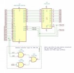
Just to recap, this is the quick and dirty solution we worked out earlier:
quick and dirty.jpg
This was tested on my HX, so it ought to work. Connecting the SRAM chip straight with A19 as enable should work as well,

The issues I was having with the '245 on my CF card, I believe, were due to cross-talk between the address and data lines, since I basically had the entire bus together in one bundle. Moving the '245 over allowed me to run a separate bundle for the data lines. Long and short of it is that even at 8-bits, on an 8088, cross-talk is an issue.

You could try adding a '245 to the card as my diagram indicates, and see if that's enough to clear it up, but those spikes make me think you could have a flaky latch as well. Is this only on select lines, or on the entire bus? Where are you measuring from?
 
Edit: Another thought -- would just removing the extra 128k of RAM turn the EX/HX into a 128k system? I wonder if it works that way. I'm curious now too! That might be the way to go if we find there is a BUS conflict... Easier if someone wants to use a single chip SRAM board without deselecting. I will test this out tonight .. my EX has zero RF shields anymore (is anyone surprised?!?) so it's easy to yank RAM chips.

I've tried pulling chips on the MB earlier this year, and on my HX at least, it doesn't work. It needs to see that onboard 256K whether it's using it or not.
 
Connecting the SRAM chip straight with A19 as enable should work as well

Yeah, it seems like it definitely should *work* even if it's conflicting with some of the built-in RAM based on my experiments with the EX yesterday. (I was kind of shocked, honestly, that the machine seemed to take having the Big Blue RAM dropped *entirely* on top of expansion RAM, including the video area, without evident complaint. I kind of want to run some more tests with sticking different values into the two respective memory banks, overlaying them, and seeing what I read back; will it be a random union of the bit states, or does one consistently win?) Whether it's safe to run like that long term is another question. It would be a shame if a configuration like that slowly wore down and killed the Big Blue chip because it and the SRAM are playing tug-of-war on every bus output in the 128k overlapping area.

A dumb idea that occurred to me, since we can't read that register, was that maybe there's a thing you could do if you really wanted to definitively know if the Big Blue chip was being programmed the same way as a "proper" 384k backfill (which is bad), or if it's entering an undocumented state to deal with a 512k backfill. The manual says that register is decoded at port 0A0-0A7h. (Looks like they're using partial decoding, not uncommon.) If you have access to a logic analyzer with enough lines you could use a '688 to decode a matching chip select for that port, and then wire up the analyzer to D0-D7, IOW and that chip select. Use the chip select as a trigger, and you should be able to record whatever gets written into that register. Then you'd be able to compare that to the documented config states and see if it's the overlapping one, the 512k+128kBB one, or some third option.

My brain-dead little 8-bit Salae Logic analyzer doesn't have enough lines to set that up properly, unfortunately.

There is one thing I know the definitive answer to. (It was brought up a while back, but this really is a thread of doom.) Radio Shack actually sold two different versions of the Plus memory adapter, the (apparently) far more common 384k model, and a second version that could accommodate 512k and came with software to use the rest of the memory as a RAM disk. We were speculating if the 512k version did exactly what the 1-chip no decoding model does, IE, give you 512k of base + the extra Big Blue memory available somewhere in an UMB using the BB's mapping registers somehow, but that turned out to not be it. The Ramdisk software that shipped with Radio Shack's board *does* work on my board that sticks the extra memory in the D and E pages, though. That may well be a piece of evidence that these machine's BIOSes don't handle 512k of base in a useful way.
 
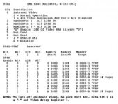
A light bulb went on in my head about how to interpret the fullest table we have for the Big Blue's register settings, so I did some more experiments. Here's the table from the TX manual:

Screen Shot 2019-10-04 at 1.31.56 PM.jpg

I realized that the address bit settings (bits 1-3 on &ha0) for the 256k Big Blue were offset by 128k from the ones for the 128k BB; IE, an EX/HX with zero K uses the same settings as a Tandy 1000A with a 128k expansion. What this means is the address bits for the "backfill positions", which are all combinations less than 100 binary, refer to the base starting position of the top 128k of Big Blue; that's all the RAM in a "conventional" 1000 and the top half of the RAM of an EX/HX; the bottom half lives under it. In a nutshell this is what I was able figure out:

First: If you toggle off bit 4 in a 1000EX it creates a memory hole from 60000-7FFFFh. The RAM page from 80000-9FFFF stays the same page it was before, IE, toggling the 256k BB to 128K *does* turn off the *lower* bank of RAM, and it doesn't move it upwards. (You can reproduce this by doing "out &ha0, &h88". Doing "out &ha0, &h98" will restore things to normal.)

This means that, yes, it is *technically possible* to make an EX/HX with a 512k RAM base expansion not contend, but the $64,000 question is whether the BIOS would ever lie to the Big Blue and turn off half of its built-in RAM to make that work. One way I suppose you could figure out is make a memory card that lets you selectively enable/disable the 128k page at 60000-7FFFF while the machine was running. (I'd suggest a 74138 or '139 and a four input AND gate with a jumper/toggle switch and pull-up resistor on the 60000h select. Boot up the machine with the RAM enabled, get into basic, toggle the switch off, and see if you have a memory hole or if you can still set/reset RAM in that area.)

Second: I was wondering if there was secret joy to be found in the undocumented settings, IE, 101 and 110. It doesn't look that way. From what I can tell from poking them in they behave the same way as 111, which is "behave like a Tandy TX". Both the 6 and 80000h pages disappeared, and no bonus RAM appeared in A0000-B7FFF either.

If someone wants to try that logic probe test the thing to look for is the state of bit 4. If the EX/HX sets that to zero when you have a 512k base RAM card installed you're fine. Otherwise not so much. You could run a trivial program at boot to set it a zero, but there's still the question of whether that would stick.
 
Yeah hi! I just have been so busy haven't had time to read here much. And yeah I wondered how you even got those connectors in the first place! I just made my connector out of a random 40 pin header and a single strip of 11 more pins ..... It's janky but it seems to work fine. Just need to make sure you align it correctly before you push it onto the connector. Ideally we would want to make a board with the SRAM, a ROM and the 8-bit CF support all on one. Way above my abilities LOL!

Btw Chaps, if you need the right andgle headers, RS have the Wurth Elektronik WR-PHD, 64 Way, 2 Row, Right Angle PCB Socket in stock - you just need to chop off 2 pins with a micro-saw.
 
Last edited:
Back
Top