• Please review our updated Terms and Rules here

IMSAI newbie, no idea what I'm looking at

found another bad socket and replaced it.

here's what I can report:

test 1/post 24:

Ok, if you look at the schematics for the front panel you should notice that all of the 7405 gates (including the address/data switches) are divided into four (4) groups driven by the signals LAD, HAD, C3 and NOOP.

The four groups are connected to a common bus going to socket U2.

A 7405 gate is an open collector inverter. As such, they do not have a pull-up to 5V. The pulls-up resistors are all on the CPU board (after U2).

First thing, after a power-up, STOP and RESET; can you measure the state of signals LAD, HAD, C3 and NOOP using your logic probe.

They should all be LOW with no pulses on them.

A LOW input to the 7405 gates should make the outputs all float. If all of the address/data switches are CLOSED, your logic probe should read all HIGH signals on socket U2.

That is the first test.

Let me know what you obtain.

Dave

CPU card in.

C3 U10-12 low
HAD U14-6 low
NOP U13-4 low
LAD U12-8 low


test 2/post 28:

Excellent.

So all of these signals LOW means that we are feeing a LOW into all of the 7405 inverters and (therefore) the output from all of the 7405 inverters should all be open circuit.

With all of the address/data switches CLOSED - this should mean that the signals on the U2 connector should all be HIGH (due to the action of the pull-up resistors on the CPU card).

Also, with all of the address/data switches CLOSED, the outputs from all of the 7405 inverter gates should also be HIGH (due to the action of the pull-up resistors on the CPU card 'feeding back' through the CLOSED address/data switches). In addition, the outputs from the 7405 inverters that do not go via a switch should also be HIGH.

Is this all correct?

Dave

all data bus LEDs on. 7405 outputs U6-4, U6-10, U6-8, U4-12, U4-8, U3-12, U3-10, U3-8 are high.


test 3/post 48:

Excellent.

With switches SA0 through SA15 CLOSED. Are all the data bus LEDs illuminated on the front panel?

Dave

all switches closed/down, all data leds on.


test 4/post 49:

If the above is correct, here is how I would proceed.

Power ON. HALT and RESET.

Set all of the switches SA0 through SA15 to OPEN. The data bus LEDs should all be ON.

Power off and remove IC U12 - observing the correct polarity of the IC within the socket for subsequent installation.

I am 'hoping' that this will cause the LAD signal to float HIGH (due to the action of the weak pull-up resistors on the inputs of the connected 7405 gates).

Power ON. HALT and RESET.

Test signals HAD, C3 and NOOP again (with your logic probe). I am hoping these three signals should all be LOW. If not, report and stop.

In theory - with the 7405 inputs HIGH (due to the signal LAD being pulled HIGH due to the internal pull-up resistors) the outputs from these 7405 gates connected to LAD should all be LOW.

By CLOSING switch SA0 - this should cause the data bus LED D0 to extinguish. The other data bus LEDs should remain illuminated.
By OPENING switch SA0 - data bus LED D0 should illuminate once again.

Repeat this test for SA1 through SA7 in turn (CLOSE followed by OPEN) and data bus LEDs D1 through D7 (respectively) should extinguish and illuminate.

If this is the case, power OFF and re-install IC U12 in the correct orientation (as found). Check for any bent pins on IC U12 after installation.

Report the results.

Dave

sw0-15 all open/on/up, U12 removed.

C3 U10-12 low
HAD U14-6 low (U4-11, U4-9, U3-13, U3-9, U1-13, U1-11, U1-9 all low)
NOOP U13-4 low

switch 0-6 toggles the data bus LEDs on/off.


test 5/post 54:

Excellent!

So, re-install IC U12 (if you haven't already) and repeat the same hassle (!) by removing IC U14 driving the HAD signal.

Make sure switches SA0 through SA15 are all OPEN.

Again, STOP and RESET.

Check that signals LAD, C3 and NOOP are all LOW.

Repeat the same process using switches SA8 through SA15.

SA8 should drive data bus LED D0 and SA15 should drive data bus LED D7 (with all of the inbetween SAn switches driving the other data bus LEDs in the same way).

Dave

U12 in, U14 removed, all switches open/up/on.

LAD U12-8 low
C3 U10-12 low PULSING
NOOP U13-4 low

switches 8-15 toggle data LEDS 0-7 on/off.


other than C3 pulsing low, I think these are all the expected results.
 
They look good.

Yes, C3 pulsing shouldn't affect the results too much. It could if it was permanently HIGH - but it isn't. Although I would have assumed that the data bus LEDs would be pulsing if they were ON - but it all depends upon the pulsing frequency of C3 as to whether you would observe it or not...

I assume in the text "switch 0-6 toggles the data bus LEDs on/off." did you mean switches 0-7 and not 0-6?

OK, put all of the ICs back in and then remove U13. Power ON, stop and reset.

This should turn all of the data bus LEDs OFF. This should activate the NOOP signal and should drag all of the U2 pins LOW.

Power OFF. Insert all ICs again and remove U10. Power ON, stop and reset.

Data bus LEDs 0, 1, 6 and 7 should be ON. Data bus LEDs 2, 3, 4 and 5 should be OFF. This should activate the C3 signal. These 7405 gates are only wired to four (4) of the common data bus lines.

Power OFF and insert all ICs again.

Retest using the IMSAI test program 1...

Dave
 
edit: going to do U13 removal test now.

but when I get to...

Retest using the IMSAI test program 1...

for clarification, continue to do this test with no RAM card installed?
 
Last edited:
post 63 tests:

OK, put all of the ICs back in and then remove U13. Power ON, stop and reset.

This should turn all of the data bus LEDs OFF. This should activate the NOOP signal and should drag all of the U2 pins LOW.

all data LEDs are off. all U2 pins are low.

Power OFF. Insert all ICs again and remove U10. Power ON, stop and reset.

Data bus LEDs 0, 1, 6 and 7 should be ON. Data bus LEDs 2, 3, 4 and 5 should be OFF. This should activate the C3 signal. These 7405 gates are only wired to four (4) of the common data bus lines.

data leds 0, 1, 6, 7 are on

but I'm a little confused by the "should activate the C3 signal" part.

U10-12 x no signal (U10 is removed)
U6-5 x, U6-6 low
U6-3 x, U6-4 low
U6-11 x, U6-10 low
U6-9 x, U6-8 low

is this the expected behavior for active C3?
 
Removing U10 should cause the C3 signal to float HIGH by the action of the weak internal pull-up resistors on the inputs of U6 pins 3, 5, 9 and 11 (7405 open collector output inverter gates).

This is what I mean by 'activating C3'. A HIGH signal level on C3 causes the 7405 inverters within U6 connected to signal C3 to drive their outputs LOW.

There are only four (4) 7405 inverters wired to drive data lines 2, 3, 4 and 5.

A low level on data lines 2, 3, 4 and 5 should turn OFF the corresponding data bus LEDs on the front panel.

The other data lines (0, 1, 6 and 7) are not driven by signal C3 and they should remain pulled high by the pull-up resistors on the CPU card.

As a result, data bus LEDs 0, 1, 6 and 7 should be ON.

>>> U10-12 x no signal (U10 is removed)
>>> U6-5 x, U6-6 low
>>> U6-3 x, U6-4 low
>>> U6-11 x, U6-10 low
>>> U6-9 x, U6-8 low
>>>
>>> is this the expected behavior for active C3?

Yes,

Your logic probe will probably report the inputs to U6 (pins 3, 5, 9 and 11) as 'X' whereas (in fact) they are pulled up high (internally) via a weak resistor that the logic probe can't see. We could (of course) used a 470 Ohm resistor on U10 pin 12 to +5V to simulate a 'real' logic HIGH - but that would have involved more work...

With a weak internal pull-up on the input of an open-circuit TTL input, the output of the 7405 inverter gate will be pulled LOW.

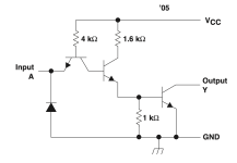
This is the circuit of a single 7405 open collector gate from the TI datasheet.

1704023774974.png
Note that the output transistor (driving signal Output Y) does not have a pull-up resistor (hence the open-collector nature of the 7405 gate).

The weak pull-up resistor I was talking about is the 4k resistor connected to the base of the input transistor (on the left-hand side). There will be a very small current flowing from Vcc through the 4k resistor and the base/collector junction of the first transistor to turn on the second transistor. There will be a larger current then flowing from Vcc, through the 1.6k resistor and the collector/emitter junction of the second transistor to turn the output transistor on, thus pulling the output to 0V.

I hope this explains the logic [no pun intended] behind what I am doing by 'pulling' the chips out that drive the inputs to the 7405 inverters?

Dave
 
Test program 1 appears to be working!! the left switches toggle the corresponding data LEDs!

I'll go through the other test and report back.

thank you so much!
 
Any other things you'd suggest trying at this point? I need to do some cleanup. Seems to be working for tests 1 and 2. back connection on old sockets seems to have been the primary problem.

test program 2.
 
Well, it was great while it worked!! I left it alone, then did some slight cleanup and reassembled the front panel and now I have a similar but different problem.

panel and CPU in, power, stop, reset. LD4 LED is off and all other data LEDS are on.

going through the steps from the previous issue:

First thing, after a power-up, STOP and RESET; can you measure the state of signals LAD, HAD, C3 and NOOP using your logic probe.

They should all be LOW with no pulses on them.
all are low.

A LOW input to the 7405 gates should make the outputs all float. If all of the address/data switches are CLOSED, your logic probe should read all HIGH signals on socket U2.

on U2, pins 4&13 are LOW. others are high.

Help me, Obi Wan!!
 
Tomorrow ok? I have given up for today.

So it seems like one of the 7405 gates driving this common line is not behaving properly.

You measured the state of the HAD, LAD etc. signals, but I suspect that one of the inputs to one of the 7405 gates is not making proper contact (through the IC socket) with the signal.

An input pin that is not making contact will float high, causing the output to pull LOW - and mirroring your described symptoms.

Can I suggest using your logic probe to look at the inputs of the 7405 gates on the chips themselves. They should be all low. I bet one will indicate as X.

Dave
 
Just looking at your original post.

U2 pins 4 and 13 being LOW does not actually equate to LED LD4.

Can you recheck please?

To save confusion, the databus LEDs are labeled as LD0 through LD7 on the schematic I am looking at.

Dave
 
LD4 stays out after power, stop, reset with CP-A and CPU in.

I went through and retested the 7405 stuff just now in this state.

C3, LAD, HAD, NOP all LOW.

U2 socket 4/13 LOW, all others HIGH.

7405 in/out are all low/high EXCEPT:

U6-10 = L
U3-8 = L
U7-10 = L
U3-6 = L

this useful? let me know what else to provide.
 

Attachments

  • led4 out Screenshot 2024-01-02 at 8.29.21 AM.png
    led4 out Screenshot 2024-01-02 at 8.29.21 AM.png
    3.7 MB · Views: 1
Excellent. Yes, all useful :)...

So I agree that LD4 is connected to U6/10, U3/8, U7/10 and U3/6. All of these being LOW indicates something is dragging this line LOW.

However, as I stated previously, this signal track goes to U2 pins 5 & 12 and NOT U2 pins 4 and 13 (according to my schematics). Is it possible you have disconnected the cable plugged into U2 (or the other end at the CPU) at some point and plugged it in backwards? Please DO NOT just reverse it without a very good reason though!

We need to isolate which gate is causing our trouble...

Can you SWITCH OFF (OPEN CIRCUIT) switches SA4 and SA12 and see what happens to LD4. This should isolate gate outputs U3/8 and U7/10 from our problem space.

Have you checked the logic state on the pins of the ICs at: U6/11, U3/9, U7/11 and U3/5? These are the inputs to the offending gate outputs.

Dave
 
However, as I stated previously, this signal track goes to U2 pins 5 & 12 and NOT U2 pins 4 and 13 (according to my schematics). Is it possible you have disconnected the cable plugged into U2 (or the other end at the CPU) at some point and plugged it in backwards? Please DO NOT just reverse it without a very good reason though!
I have not reversed the connector. figured it out early on and the orientation is pretty clear in that the ribbon comes out of the top side of the CPU with red to the right. when I had the machine functioning it was in this position also.


We need to isolate which gate is causing our trouble...

Can you SWITCH OFF (OPEN CIRCUIT) switches SA4 and SA12 and see what happens to LD4. This should isolate gate outputs U3/8 and U7/10 from our problem space.
with 4 and 12 up/open/on does not change anything.

Have you checked the logic state on the pins of the ICs at: U6/11, U3/9, U7/11 and U3/5? These are the inputs to the offending gate outputs.

Dave

all 7405s are low in, high out except the ones I noted.
U6-10 (input, labelled incorrectly on schematic) L
U3-9 L
U7-11 L
U3-5 L
 
Not quite making sense I am afraid at the moment...

Can you make sure that ALL of the address switches SA0 through SA15 are switched so they are OPEN circuit please. Double check (with the power OFF) that this is the case with a multimeter.

That should rule out the 7405 inverters driven from the HAD and LAD signals.

Dave
 
Back
Top