• Please review our updated Terms and Rules here

Info about Model I piggyback board HEIIB006000

HansTRS

Member
Joined
Sep 9, 2023
Messages
18
Location
The Netherlands
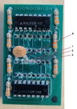
My TRS-80 Model I (manufactured in Japan) board has a piggyback board with code HEIIB006000 as shown in the photo. It contains 2 74LS157 chips, 7 resistors and 1 ceramic capacitor. Unfortunately I can't find any documentation about it. Can anyone tell me what this board is for?

The board has been sloppy soldered, points 1, 2 and 3 (image) do not appear to be connected to anything. Maybe point A should be connected to point 1, but I can't judge that.

I hope someone knows more about this and can help me.
PiggyBack.jpg
 
What does the other side look like? Where does it go?

74LS157 is quad 2-to-1 mux, so it's 8 bits of multiplexing... something.
 
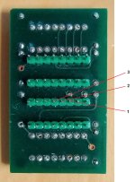
Here is a photo of the bottom, as you can see it seems that points 1,2 and 3 are not connected to anything, but I would like to be sure.

Under a microscope I saw that the ceramic capacitor does make contact via copper paths that are difficult to see (top of the PCB), so that seems OK.

bottom.jpg
 
Yes, and where does it go? Are there two empty IC sockets on the motherboard for it? It's clearly changing or adding to some existing circuit. Those pins aren't used because they weren't used by the original chips that this is patching around.
 
If what you write is correct that the pins are not used, my board will be fine.

The board plugs into Dupont female headers on the motherboard, Z13 and Z14, both marked LS157. It looks like it was originally applied during production (in Japan). However, I haven't seen this anywhere in documentation or on the internet, so if anyone has experience with it or a schematic, I'd love to hear it.
 
Z13 and Z14 on the tech manual schematic are 16K DRAMs. They are served by Z35 and Z51 which are both LS157, but those are in vertical orientation on a standard Model I. So it's for a different motherboard. (I'm guessing it's one that someone posted a picture of here a few months ago.)

What I suspect is that there was something wrong about the way the LS157s on the board were wired up. First of all, only 7 of the 8 muxes are needed for 16K (which is why the unused 3 pins), and you can see that a lot of the traces link up corresponding pins between the sockets and the chips.

The interesting part is the resistors on the board. There are seven of them, and they are probably 33 ohms (I really hate resistor color paint in ambiguous shades, that black looks almost brown), which is rather common in-line with DRAM address lines. I'm going to guess that the "patch" was to insert the resistors to the DRAM address lines to increase reliability, possibly due to a particular type of DRAM chip having problems.

So literally it just inserts resistors to the outputs of the DRAM address muxes. This wouldn't be the first time I've seen a daughterboard that simply improves the quality of chip output signals.
 
Z13 and Z14 on the tech manual schematic are 16K DRAMs. They are served by Z35 and Z51 which are both LS157, but those are in vertical orientation on a standard Model I. So it's for a different motherboard. (I'm guessing it's one that someone posted a picture of here a few months ago.)

FWIW, Search for “Japanese TRS-80 manual” and the first hit on archive.org is the service manual for the Japanese TRS-80s. The parts list confirms Z13 and Z14 are ’157s.
 
The motherboard is Japanese, I don't find as much about it on the internet as the other models. The code TEC HEIIE011510 is printed on the board. The 7 resistors on the daughter board are 330 ohms, the colors in the photo are indeed difficult to see. Originally there were probably 2x LS157's soldered in that place. It now seems that the daughterboard is otherwise OK, I will now continue to investigate why I only have random characters on the screen.

@Eufimorphodon
I had previously downloaded the manual for the Japanese version, unfortunately the scan of the diagrams in that PDF is not good, there are many black spots. Were you able to find the diagram(s) without those spots? The daughterboard is not described or shown in the manual I downloaded.

PS: Because the moderator has to approve my postings in advance, there is a delay in my responses.
 
Back
Top