• Please review our updated Terms and Rules here

Intel iSBC 386/AT or MicroSystem/AT 301 motherboard jumper settings

mR_Slug

Veteran Member
Joined
Nov 28, 2006
Messages
941
Location
UK
Hi i have a very old 386 16MHz Intel motherboard:
attachment.php


I am trying to install a proprietary memory card into it. The problem is I cant find the jumper settings to set the memory size. It has phoenix BIOS dated '86. I have tried a couple of utilities to set the BIOS settings, and the extended memory size, but neither work.

Memory card:
attachment.php


I have found a manual for the Intel 302 system/motherboard, that was the next model on. This allowed me to get the weird Serial port header pin out, however the jumper settings are completely different. This model requires that the memory size is set with jumpers, so I'm assuming the previous model, that i have, requires this too.

I have searched everywhere for the manual to the motherboard, and it isn't online, or even anywhere to buy AFAIK.

This is a very early board and, like the IBM AT, does not have a chipset as such. If someone has the manual, that would be great, it is not in TH99. Failing that, does anyone have any idea what chip is likely to read the jumper settings in relation to the memory size. 8237A DMA chip? I'm trying to decipher what the jumpers do, and would like to home in to the right set if possible.

Or failing that, does anyone know what the memory size jumpers on the IBM XT are connected to? IIRC the AT does it in BIOS setup.

Any help appreciated.

Andrew
 
This model requires that the memory size is set with jumpers,
That has to be an assumption, because you do not have access to the manual. The motherboard jumpers could be for other things (e.g. serial port enable/diable, parallel port enable/diable, serial port address, ...)

Or failing that, does anyone know what the memory size jumpers on the IBM XT are connected to? IIRC the AT does it in BIOS setup.
In the IBM AT (and many clones), the BIOS SETUP does not set/configure RAM. The RAM figures put there are indicators to the Power On Self Test as to what RAM should be found at power-on.

I have searched everywhere for the manual to the motherboard, and it isn't online, or even anywhere to buy AFAIK.
Whilst not a manual, there is a "MICROSYSTEM/AT 301Z" described on pages 1-7 and 1-8 of the document at [here].
2 MB of RAM on the motherboard.
Optional memory cards: 2 MB or 8 MB.

Is your system a 301 or a 301Z ?

Regarding your RAM card. If the RAM chips on your memory card are 41256-class, then you have a 2 MB card. There are no jumpers/switches on the card, and I do not see any 'intelligence' on the card. Therefore, it most likely sits at a fixed address.

From the photo, it appears that the motherboard does have RAM on it (lots of the same looking chip grouped together). I suggest that you tackle the issue in two steps.
Step 1: Put the memory card aside and just get the motherboard going/configured on its own.
Step 2: Add the memory card, adjusting BIOS SETUP appropriately.

For step 1, assuming that there is 2 MB on the motherboard, I think it likely that the engineers would have divided it per either:
* 512 K of base memory, plus 1536 of extended memory.
* 640 K of base memory, plus 1408 of extended memory.
 
We used lots of these Intel 301 boxes, I never remember jumper settings for memory. There is only 512K memory on the motherboard, just set the expansion board to start at 512K. The 301Z is completely different, it used the SX CPU. The 302 is also totally different with a 25MHz CPU and 1MB (more than 512K anyway) on board.
 
That has to be an assumption, because you do not have access to the manual. The motherboard jumpers could be for other things (e.g. serial port enable/diable, parallel port enable/diable, serial port address, ...)
In the IBM AT (and many clones), the BIOS SETUP does not set/configure RAM. The RAM figures put there are indicators to the Power On Self Test as to what RAM should be found at power-on.

Yes it is an assumption. I've based it on the manual for the next model, the 302. If I insert the card (either slot) there is no difference to the ram count at start up. So either:
1. it is defective,
2. The ram has to be set in the bios (unlikely, as the board is designed to be AT-like, and 2 different utilities didn't work)
3. The ram size has to be set on the motherboard
4. the ram size is set automatically, but a jumper has to be set to indicate that there is extended ram to count.

As, i cant test if its defective, and setting the ram size in the bios setup programs didn't work, i am currently looking at jumper settings.

Yes i have the 1989_OEM_Boards_and_Systems_Hanbook.pdf, not a huge amount of info in it unfortunately. I have the basic 301, not the 301z. It is also an early revision, and wont support the 8MB ram cards. Actually it wont support the 387 NPU, or even run 32-Bit code correctly due to the CPU. It's the greatest 386 ever!

I have the 2MB card.

Regarding the memory config, the board is weird. there is 512KB ram on board. This works fine.

As woodchips points out, the extended ram card start at 1024KB. 512KB-640KB can only be filled with a 16-bit AT bus ram card (according to an Infoworld article). It is a bit of an odd design decision. There is no support for bios shadowing, so filling from 512K to 1024K, in a contiguous configuration, and putting the rest into extended is wasteful. This kinda makes the design seem a bit more logical, but I would have thought adding 640K on the board, or allowing back-fill would have made more sense. Perhaps they didn't want to interfere with EMS cards? I cant see why they couldn't make it all work together, but for whatever reason they didn't.


So I am past step 1, the motherboard ram works fine.
step 2, is problematic, :)

I found a picture of the motherboard on the web, and even though it was pixelated i was able to just about make out a different jumper setting configuration. I tried it, but no cigar. I have cautiously tried removing some jumpers and powering it on but nothing not even less ram.

There are 3 main jumper locations i am currently looking at:

Firstly, the board does not label jumpers, like JP2, jp3 etc, instead it labels pins:

First location, (in the red box) see attached image:

Code:
     ------      ------
E37  |*--*| o  o |*--*| E42
     ------      ------
        ------------
      o |*--*||*--*| o  o
        ------------


Second location, (in the green box) :

Code:
         o  E19

        ---
        |*|
        |||
        |*| E21
     ------    
E22  |*--*|
     ------
      o  o
   
E26   o  o  E27


        ---
        |*| E28
        |||
E29   o |*| 
        ---    
      o |*|
        |||
      o |*|
     ------
E35  |*--*| E36
     ------

As you can see these jumper configurations, are not simple set, no set configurations, It appears to me that for example the jumper from E35 to E36 can be removed and 2 jumpers installed vertically, going from ?E33? to E36 and ?E34? to E36.

jumpers.jpg (Image contains jumper locations, and some chips are labeled)


I would like to try to narrow down what jumper does what. Or at least determine that it is cannot be to do with some jumpers. Serial parallel are set elsewhere up near the keyboard connector AFAIK. the Color/Mono jumper is Definitely set elsewhere.

So If you were to take a hypothetical motherboard that needed to be told what size ram it had installed via jumpers, what chip would this jumper be connected to?

Sorry for long post, but damn this is confusing.
 
As woodchips points out, the extended ram card start at 1024KB. 512KB-640KB can only be filled with a 16-bit AT bus ram card (according to an Infoworld article). It is a bit of an odd design decision.
No different to the IBM AT. 512KB-640KB provided by way of their optional '128KB Memory Expansion Option' card.

I figure that it was because of limited real estate on the motherboard.

So If you were to take a hypothetical motherboard that needed to be told what size ram it had installed via jumpers, what chip would this jumper be connected to?
The engineer has a few choices. As one example, per the IBM AT diagram at [here], the IBM engineers chose to use spare input/output pins on the keyboard controller.

I would like to try to narrow down what jumper does what. Or at least determine that it is cannot be to do with some jumpers. Serial parallel are set elsewhere up near the keyboard connector AFAIK. the Color/Mono jumper is Definitely set elsewhere.
You may end up having to work out parts of the motherboard circuit diagram.

Even that sometimes is not enough. An example is the diagram that I pointed to earlier. The fact that J18 connects to an input/output pin, pin P14, on the keyboard controller does not inform me as to the function of J18. Code (including the BIOS) has the ability to read the state of pin P14, and thus the state of the J18 jumper, but the J18 purpose can only be learned by:
* Technical/user documentation; or
* Observing a change in motherboard behaviour when J18 is adjusted.
 
How did you determine that this is an iSBC board?

Thats what it is referred to in the 1989 OEM PDF that modem7 posted. (And also some infoworld articles)

The intel part no for the manuals are:
149565-002 iSBC 386 AT User's Guide
280736-002 iSBC 386AT Product Profile

It was used in these systems:
Computer Dynamics Micro System 386
PC Discount Nobel 386
Corvus 386
Kaypro 386
Laser Digital 386
CAE/SAR 386
Micro 1 386 PC
Osicom 386
wang 380

Unfortunately cant find any manuals relating to those systems either:-(

\/ \/ \/ This isn't a rant, looking back I kinda find it humorous to the effort I have gone to to build this system.
Every time i try to do anything with this board, it takes me on a wild goose chase. I bought it of ebay.de, and i had to do a bank transfer to pay for it. I rang eBay about payment and they told me I could do PayPal to SWIFT. Well, long story short, that turned out to be nonsense. Bank charged be ££ to do bank transfer. BTW i have used TransferWise since then, way cheaper.

Then I tried to find full AT case, this took weeks of searching, finally found one, got it, and the PSU was broken. See this thread:

http://www.vcfed.org/forum/showthread.php?50260-AT-PSU-repair

Thanks again everyone for the help. So then I give up and hack up an LPX style small "standard" AT PSU, (Same size as ATX), and put it inside the AT PSU. This all works fine. But now there is a weak connection in one of the motherboard power connectors on the PSU. (My own fault, i know whats wrong).

Then i go to install the motherboard. Full AT boards require little C-shaped, plastic stand-offs on the right side nearest the PSU. This was a wild goose chase in of its self from a previous system I built. Luckily I found a company and bought 50 of them. This motherboard/case has 2 actual screw standoffs, the previous owner had removed one. So I had to fix that too <sigh>. Then I had to track down the Serial header pin-out. This i got from the model 302 manual. Took almost 4 hours just to figure out the serial port connector!

All this to have one of the slowest 386's with no cache, with no ability to work with a 387, with an absolute maximum of 4MB ram, that cant even run 32-bit code correctly:)

Really any help appreciated at the moment. Anyone have any luck with reverse-engineering jumper settings? And anyone know what chip is likely to be associated with extended ram count?
 
You don't have an extended memory card elsewhere that you could try in one of the 16-bit slots ?

That is a very elegant solution to a problem, I wish i'd thought of that. yes i do have one. I
've Been probing away, discovered some jumpers purpose, its late here now, so i will have to continue tomorrow.
 
No different to the IBM AT. 512KB-640KB provided by way of their optional '128KB Memory Expansion Option' card.

I figure that it was because of limited real estate on the motherboard.

This certainly makes sense on the AT with a 16-bit bus, However on a 386 with a 32-bit memory bus, There is the first 512KB with 32-bit access. Then 128KB with 16-bit access then, from 1024KB onwards 32-bit access. IF something like say OS/2 is unaware of the slow 128KB range, AFAIK it will slow down things a bit.

To me it would have made more sense to either have the 32-bit card back-fill down to 512KB or somehow put 640KB on the board. The only reason that i can see apart from cost or space, is possible conflicts with expanded memory. It has been a long time since i dealt with Expanded RAM, so i may be completely wrong on this. I seem to remember there were 2 ways of installing it, and one was called "large-frame" or something.

The engineer has a few choices. As one example, per the IBM AT diagram at [here], the IBM engineers chose to use spare input/output pins on the keyboard controller.

You may end up having to work out parts of the motherboard circuit diagram.

Thanks, that is the sort of thing i was looking for. However "The engineer has a few choices" is what i was afraid you'd say.

I have worked out some Jumpers. Found IRQ assignments for Serial/Parallel and thanks to your? minuszerodegrees.net site, I think i have loosely figured out the parallel printer circuitry. It appears to be the same as the IBM Serial/Parallel Adapter. The Serial was easy to figure with the NS16450N chip. One thing I cant get is continuity between the IRQ jumpers and the NS16450N. The parallel circuitry is a little different, or at least the place where I thought the IRQ pin should be is different.

Also I think i have the NPU enable and "bios ROM size" jumpers identified.

The fact that J18 connects to an input/output pin...

I am currently poking around the keyboard controller. There is a simple 3 pin jumper next to the Keyboard connector, but this has no effect on the memory card.

You don't have an extended memory card elsewhere that you
could try in one of the 16-bit slots ?

I Pulled an IBM 128KB/640KB Memory Expansion Option (128 populated) and an Intel "Classic" ram card out of an AT I have. Both seem to work, the ram counts up fine. It never really crossed my mind to to try that. I tried the system with the 128KB card, and the 32-bit "MEM020" ram card, but no count beyond 640KB.

I think I'll still have to check those jumpers, as the 32-bit ram card *may* operate differently. For example there may be a jumper that sets whether ram above 1MB is on the AT bus or on the 32-bit bus. Unless anyone has any other ideas?

This is a very frustrating computer, although very rewarding every time I find continuity between 2 points, I keep saying Yay!
 
No different to the IBM AT. 512KB-640KB provided by way of their optional '128KB Memory Expansion Option' card.
I figure that it was because of limited real estate on the motherboard.
This certainly makes sense on the AT with a 16-bit bus, However on a 386 with a 32-bit memory bus, There is the first 512KB with 32-bit access. Then 128KB with 16-bit access then, from 1024KB onwards 32-bit access. IF something like say OS/2 is unaware of the slow 128KB range, AFAIK it will slow down things a bit.
You are right. I forgot that we are dealing with a 386.
 
Hi, I've been probing away and I seem to have workout some of the jumpers. One jumper I am trying to eliminate from the memory configuration is a 3 pin jumper next to the keyboard connector:
Code:
        ---
        |*| E1
        |||
        |1| 
        ---    
         1  E3
E1 goes to pin4 (RESET) of the keyboard controller.

Both E2 and E3 are connected together regardless of jumper configuration and connect to pin 3 of the keyboard connector. Which is supposed to be not used by the keyboard. I have tried to find another place on the motherboard that has continuity to this, but as of yet no luck. It does not stop the no keyboard present error. Anyone have any idea?


Back to the memory, I have decoded some jumper settings related to the ram:
Code:
        ---
        |1| E28      G = Ground
        |||
E29   G |1|          1, 2, 3 = Numbered pins have
        ---    	     continuity, with pins of the 
      G |2|	     same number. This holds true
        |||          whether the jumpers are ins-
      G |2|          talled, in the configuration
     ------          shown  to the  left,  or re-
E35  |3--3| E36      moved.
     ------
The only other jumper configuration that makes sense AFAIK is:


Code:
         1  E28      G = Ground
     ------
E29  |G--1|          1, 2, 3 = Numbered pins have
     ------    	     continuity, with pins of the 
     |G--2|	     same number. This holds true
     ------          whether the jumpers are ins-
     |G| 2           talled, in the configuration
     |||             shown  to the  left,  or re-
E35  |3| 3  E36      moved.
     ---
I've not experimented with connecting groups 1 to 2 and groups 2 to 3.

Adjacent to this jumper block is a 916C103x2PE chip. AFAIK, this is a DIP resistor network. E28 and E30 lead to pin 5 of this chip. E32 and E34 lead to pin 6, and E35 and E36 lead to pin 7. Cant find a datasheet for this chip.

With the memory card in J19 (the slot on the left), Connecting E29 to E30 produces this message on boot up:

data line failure at 100000-10FFFF

Adding either, or both of the other jumpers in the configuration above produces the same result. With E29-E30 removed, the system does not report any memory error, nor count any extended memory. If I install the memory card in J20 (the slot on the right) the jumpers seem to have no effect.

So from this I am guessing that I have managed to enable the memory card, and found the first slot, but it seems to have an error in the first 64K?

Occasionally i get this message on bootup:

Memory write/read failure at 100002, read FF30 expecting FF10.

At present, this error seems like an intermittent problem. I cant easily reproduce this error. With either error, it would appear that there is a faulty ram chip on the memory card.

The chips are labeled TMS4256-12XL so they are 41256 class. At present all i know about the ram card, is that the configuration is interleaved.

Does anyone know which chip may be located at 100000h? Or failing that how to work out which chip is located at 100000h? Anyone have any experience with this sort of thing? I am at a loss to know where to start. Bear in mind all the RAM is soldered down, limiting my options a bit. Is there a way to test soldered ram chips?

Thanks

Andrew
 
I asked Chuck McManis about this, and I will quote: "Andrew, the poster doesn't seem to realize that there are 16 (or 32) chips at location 0x100000 (1MB) according to his last entry on the board.
 
I'm not sure how long is too long to revive an old thread. But here goes anyway. Please let me know if its better to start a new thread.

I have had a few questions PM'd to be about this system and I was eventually able to get the thing working. The short answer is that I worked out the functionality of the RAM card and still ended up mass desoldering chips using a paint stripper gun and socketing them. It's now working. I plan to document the board in some detail in the future. It will be along the lines of the Ardent Tools of Capitalism pages for the PS/2's.

@yuhong - My question "Does anyone know which chip may be located at 100000h" was a bit sloppy.

The long (rambling) version:
The board responds in 32-bit chunks, or 64-bits (32-bit chunk followed by another, it's interleaved). So given an input address with a RAS+CAS format, IIRC first the board responds with all the bits from the chips on the right giving 32-bits, and 60ns later does the same with all the chips on the left.

However before probing LITERALLY EVERY SOLDER POINT:) I didn't know how the physical RAM layout mapped to the logical one. It seemed reasonable to say that all the chips on one side were accessed first, followed by the other side, but I didn't know for sure. It could have been some other configuration.

The board is effectively addressed in 64-bit chunks. change one bit in the address sent with the RAS or CAS, and the board responds with a new 64-bits sent in 2 32-bit groups.

the "Memory write/read failure at 100002, read FF30 expecting FF10." gives indication that the BIOS message is numbered in bytes. 100000h is 1024KB. So 100000h refers to the first byte, 100001h second, 100002h third and 100003h fourth. The error "read FF30 expecting FF10" along with "100002" gives indication that the bios is counting in words. So 100000h refers to the first word 100002h the second. That is, it's never going to respond with the message "Memory write/read failure at 100001..." It's only ever going to show an even number.

Confusion #1: numbering in bytes, counting in words. To an ASM hacker, this is entirely logical when you consider the AL AH AX registers. To a simpleton trying to replace a RAM chip, it's confusing.

So from this we can determine that at address 100000h there are only 8 chips. (lets forget the interleaving for the moment)

There is still a problem of which 8 chips? and of those 8 which is bad?
Code:
FF30 is: 11111111 00110000, and 
FF10 is: 11111111 00010000, xor'd giving
         00000000 00100000
and this all starts at 100002h. So looking at it from a 32-bit perspective, at 100000h:
Code:
00000000 00000000 00000000 0010000
Confusion #2: numbering in bytes, counting in words, with a dword interface. To an ASM hacker, this is entirely logical when you consider the AL AH AX EAX registers. To someone realizing they're out of their depth, trying to replace a RAM chip, it's confusing.

Confusion #3: By the way it's interleaved! <facepalm>

So now we have:
Code:
00000000 00000000 00000000 00000000 00000000 00000000 00000000 00100000 or perhaps:
00000000 00000000 00000000 00100000 00000000 00000000 00000000 00000000
On top of this I didn't know which bit was the LSB, so you could inverse the two previous patterns. And on top of that there are also parity chips. So if we try mapping this to the card. Lets assume all the parity chips are on the bottom, and the LSB is the top left we can mark an x on the bad chips matching each of these patterns. Problem is maybe the LSB is the the bottom right, or maybe it starts at column 4 at the top (or bottom), maybe it counts from column 4 at the top to column 1, or perhaps the parity bits are at the top transposing my x marks the spot pattern one chip up. Essentially what I came up with was this:
Code:
P? = Parity?  x = Likely spot  ? = possibility
 ______________________________________________________________________________________________________  ___
| _____   _____   _____   _____      _____   _____   _____   _____      _____   _____   _____   _____  ||
||_P?__| |_P?__| |_P?__| |_P?__|    |_____| |_____| |_____| |_____|    |_P?__| |_P?__| |_P?__| |_P?__| ||
| _____   _____   _____   _____      _____   _____   _____   _____      _____   _____   _____   _____  ||				
||_____| |_____| |_____| |_____|    |_____| |_____| |_____| |_____|    |_____| |_____| |_____| |_____| ||
| _____   _____   _____   _____      _____   _____   _____   _____      _____   _____   _____   _____  ||				
||__x__| |__?__| |__?__| |__x__|    |_____| |_____| |_____| |_____|    |__x__| |__?__| |__?__| |__x__| ||
| _____   _____   _____   _____      _____   _____   _____   _____      _____   _____   _____   _____  ||			
||__x__| |__?__| |__?__| |__x__|    |_____| |_____| |_____| |_____|    |__x__| |__?__| |__?__| |__x__| ||
| _____   _____   _____   _____      _____   _____   _____   _____      _____   _____   _____   _____  ||				
||_____| |_____| |_____| |_____|    |_____| |_____| |_____| |_____|    |_____| |_____| |_____| |_____| ||
| _____   _____   _____   _____      _____   _____   _____   _____      _____   _____   _____   _____  ||				
||__x__| |__?__| |__?__| |__x__|    |_____| |_____| |_____| |_____|    |__x__| |__?__| |__?__| |__x__| ||
| _____   _____   _____   _____      _____   _____   _____   _____      _____   _____   _____   _____  ||				
||__x__| |__?__| |__?__| |__x__|    |_____| |_____| |_____| |_____|    |__x__| |__?__| |__?__| |__X__| ||
| _____   _____   _____   _____      _____   _____   _____   _____      _____   _____   _____   _____  ||				
||_____| |_____| |_____| |_____|    |_____| |_____| |_____| |_____|    |_____| |_____| |_____| |_____| ||
| _____   _____   _____   _____      _____           _____   _____      _____   _____   _____   _____  ||				
||_P?__| |_P?__| |_P?__| |_P?__|    |_____|         |_____| |_____|    |_P?__| |_P?__| |_P?__| |_P?__| ||
|______________________________________________________________________________________________________||
                                      |_____________________________||___________________________|      |
IIRC they're 14 pin dips so, that's at the very least 16 X's 14x16=224 pins to desolder. Say I find the right chip half way thru, that's still over 100 pins to desolder. There's no way I can possibly remove 100 pins without destroying a solder pad leaving the board in a state that just has more variables leading to non functionality. But the problem could be with a parity chip? Or perhaps the chips physical layout don't map consecutively to the bit pattern (the ? marks). So even if I do all this without screwing up once, it still may not work. On top of all this I'm not 100% sure my reasoning is sound, it *seems* rational. But there is always the possibility I'm a crazy-person with the delusion that I *seem* rational. I mean I have just but a paragraph ago created an ASCII-art diagram of a memory card.


So I decided to workout the entire schematic of the memory card:
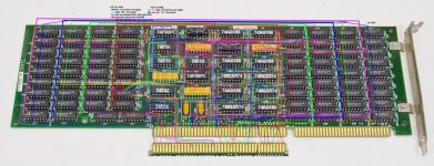
board(all).jpg

And then worked out the logic of the card. I've still got all the notes, but it is far from an easy to understand description of the card.

This was an interesting exercise, but not terribly fruitful. I discovered The parity chips are at the top. Also the chips on the right are read as the first 32-bit word followed by the left chips. On the right set of chips, the one at the bottom left, has its data pin connected to the first pin (component side) of the memory connector. The chip above this is the next pin, and so on. So either this is the LSB or the MSB. On the left side the arrangement is inverted. So the LSB/MSB is the bottom right.

So then I tried to use the pinout of the 386 to track back to the memory card to workout what was the LSB and the MSB. I got lost at some tri-state chips, and the process started to become very complicated.

I then looked at alternative ways of desoldering chips, and I ended up using a paint stripper gun. There is another RAM card in existence, so worst case I would order another. In hindsight it would have been much quicker to start with this, but I've at least gained a better understanding of this system. My first plan was to remove a column of RAM, socket them, then test. I was running out of DIP sockets, so next I removed some rows of chips, socketed them, and bingo, now I had an error in a different place. Some switching around and I found the faulty chip.

Anyway it all seems to be quite happy now. Only thing now is some of the chips in the dip sockets still have some solder on them, so some work loose occasionally.
 
Thanks. But I had already found that manual. It was useful in working out the serial port header.
 
Hi anybody. Sorry for necroposting.
I have this motherboard: "SSBC 386AT", "PBA 451213-004" "SND108852". Such motherboard as at mR_Slug.
I also have 2M RAM board: "ASEM 2MB 386".

My jamper:

Code:
     ------      ------
E37  |*--*| o  o |*--*| E42
     ------      ------
     ------   ------
     |*--*| o |*--*| o  o
     ------   ------
Secon jamper location:
Code:
         o  E19

           
         o 
           
         o  E21
         
E22   o  o
      
      o  o
   
E26   o  o  E27


         o E28
         
E29   |*-*| 
             
      o |*|
        |||
      o |*|
     ------
E35  |*--*| E36
     ------

Next group:
Code:
E13 |*-*| o
    o |*-*| E18
Motherboard see extended 2048 RAM. But I have another problem. Motherboard no wont boot from FDD. In the BIOS I have set 1.4MB type of fdd. It jerks the head of the drive аnd rotates the disk endlessly. FDD, fdd controller and floppy have checked on other system.

What do you think might be the problem? Maybe I need a special drive controller? Or SCSI?
 
Anyway it all seems to be quite happy now. Only thing now is some of the chips in the dip sockets still have some solder on them, so some work loose occasionally.

Photo of my board (photo from internet, but it identical):
file.php
file.php

My jumpers is different with your configuration. And by default, in the far slot (from the processor), the memory card was seen (determined by the motherboard) immediately, and in the BIOS there was an indication of the size of the expanded memory 2048. True, there was an error about "Memory write/read failure at ****, read **** expecting ****".
But I am interesting, without RAM card is motherboard boot from floppy or not? What floppy do you have (try to boot from)? What type of FDD controller? Is 512k of built-in memory enough for boot ?
My motherboard - not wont boot. It is hangs after self-test, spins the drive spindle endlessly (not sense for Alt-Ctr-Del).
Do you have the opportunity to make a copy of the BIOS? (It is always useful to have a backup copy of the bios, the time is not spare (favour) charges in the ROM's crystal )
(I am not native language speaker, for information ).
 
If someone can make of the copy of the BIOS, could they send it to me? I've still been unable to verify whether the BIOS on my board is functioning. The original BIOS doesn't work, and I've also tried the copy hosted here, and have correctly set the jumpers to accomodate the 27512 chips needed, but have been unable to get the machine working. The BIOS hosted in Vogons also seems a little sketchy, since it is a pair of 64KB chips instead of 32KB ones, and the low and high halves were mislabeled as each other...
 
If someone can make of the copy of the BIOS, could they send it to me? I've still been unable to verify whether the BIOS on my board is functioning. The original BIOS doesn't work, and I've also tried the copy hosted here, and have correctly set the jumpers to accomodate the 27512 chips needed, but have been unable to get the machine working. The BIOS hosted in Vogons also seems a little sketchy, since it is a pair of 64KB chips instead of 32KB ones, and the low and high halves were mislabeled as each other...

If I find my Willem device (this may take a while, the point is, I do not remember where I saw it last time, and also need to remember how to work with it), I will make a copy of the BIOS.
But I'm not sure that my good BIOS, the motherboard does not boot from the floppy disk.
 
Back
Top