• Please review our updated Terms and Rules here

Junk bin ZX Spectrum board

ajcc

Experienced Member
Joined
Aug 22, 2009
Messages
159
Location
Karlstad, Sweden
Hi guys!,

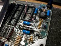
A while back I saw a board with a Sinclair logo on a bare board, among a bunch of old PC-gear, and I decided right away that I had to have it! It was missing IC's, and I found out some parts are broken and PCB traces might be damaged. At least the Z80, the BASIC ROM and the Ferranti ULA is there, so if they are working... maybe there's still hope.

I was lucky to find the schematics for this Issue Two ZX with a lot of detailed notes at a blog called: L BREAK Into Program, 0:1 (http://wordpress.animatez.co.uk/computers/zx-spectrum/hardware/).
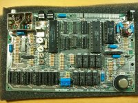
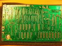
100_1166.jpg

100_1167.jpg

First, the missing IC's:
IC25: 74LS157 - Quad 2-Line to 1-Line Data Selector/Multiplexer
IC26: 74LS157
Both used for addressing the upper 32k of memory, each addressing 4-bits of the 8 address bits.
The lower memory is hooked directly to the ULA and a second set of 74LS157s to interface them to the common CPU bus.

IC23: 74LS32 - Quad 2-Input OR Gate
Used along IC24 (74LS00, Quad 2-Input NOR Gate) for DRAM, Column, Row and Read/Write access.

It's also missing 5 out of 8 lower DRAM ICs, D416C.
And the 7805 linear regulator.

There's a Cap (C35) and Diode (D13) cut off next to the tape in/out jacks.


Anyway, that's just the first look. While the missing 74-series logic could be replaced easily. The RAM might be harder?, I've never worked with DRAM, or any RAM outside uC's, before.

More as it happens!
 
Short update: I have been trying to read the content of the ROM with my EPROM-programmer, and it's only giving me FF, same as with no IC inserted in the reader. So it might be dead. Using Deoxit Spray on the legs didn't solve this either.

ROMs could be replaced. Next step is testing the Z80 I guess.
 
Nice find!
Do you have the pinout for the ROM? It could be that it's not pin-compatible with the corresponding EPROM, though on the spectrum+2, it is.
The RAM shouldn't be that hard. Haven't worked too much with DRAM either, but the D416C seems to be the NEC equivalent of the 4116 DRAM, and I know I've seen that for sale.
This is the datasheet 4116: https://console5.com/techwiki/images/8/85/MK4116.pdf
and the D416C: http://www.datasheet4u.com/datasheet/D/4/1/D416C_NEC.pdf.html

Atleast the pinout is identical.

Good luck with the restoration!
 
Hi guys!,

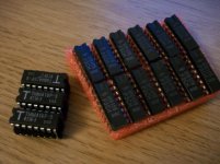
It's been quite a long time since I have made the last update on this junk-bin board. But lately I've bought a few junk-bins of logic ICs off eBay and in the last box that I bought, these little ICs was included:

100_3052.jpg

Those are indeed 4116 and 416 DRAMs, albeit 300ns instead of the 200ns ones currently on the board. The strange thing is that the legs of the 4116 ICs are really oxidized, not sure if that's a common thing or a sign of something bad? Those DRAMs of-course got me thinking about the ZX board again! And I see that I never posted an update about how I tested the Z80 CPU:

100_2821.jpg

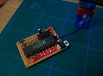
Nothing, apart from getting warm... quite warm. So to test my tester I bought another Z80, which (sadly?) worked very well (I have since bought yet another one). At this time it was clear to me that I needed a battery powered Z80 CPU tester. The tester is based on Thomas Scherrer's classic circuit, with a lot more LEDs, too many actually. Which taught me to only read the Address bus when it's stable. So funny enough, this is why I ended up buying people's old junk-bins of ICs from eBay.

100_2880.jpg

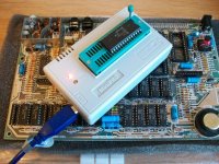
Forward to today when I decided to set up and try to read the PROM again. Sadly it was still the same all 0xFFs (blank, or just dead). The miniPRO reader doesn't have a HN613128P in the list of known devices, but it does have the UPD27C128. It's a common 27C128 that's pin-out compatible (with previously mentioned Hitachi PROM) and was used on some ZX Spectrum boards, at least some that I saw when trying to identify missing parts of my Issue Two board.

100_3042.jpg

OK. Now what do we do? Well, there's a single socketed 74LS00 Quad NAND-gate on the board, those are easy enough to test! It took a second or so before I had come to senses and realized that the default output is indeed a Low signal (if you are unfamiliar with 74-logic, they have internal pull-ups, NOT High AND High is a Low putout signal). So that one seems to be working happily enough.

100_3046.jpg

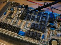
Wondering if I could test something else and being worried bout the state the ULA is in. I decided to just go for it, to check and see if there were any Clock signals at all.

100_3050.jpg

And... there was, one.

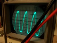
100_3049.jpg

That's the output on pin 32, CLK. The clock signal that goes off to the Z80. Which is supposed to be 3.5-something MHz and it doesn't look completely impossible that it would be. The scope was set to 0.1uS divisions. But there's one alarming thing...

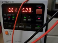
100_3051.jpg

There's almost no ICs on the board and yet it is pulling 600mA with the ULA being too warm to touch. I did notice it quickly and only ran it for a few seconds, so I hope it didn't make the problem worse. There was or might still be something that killed a Z80 and a PROM on the board, possibly a few DRAMs and some 74-logic too?


So that's where I'm at with this junk-bin board. The PROM I could burn a new one, I have a least one 27C256 EPROM. It has an identical pin-out except an extra address line where the /PRM pin is on the 27C128.

But the real concern is, as most of you will understand, the unknown condition of the ULA. Maybe one could try to get the different sync signals out of it on a breadboard? It would be nice to test it outside the board, don't know if there's an issue with the board. There are some missing components that I will have to identify, so at least I will have to go through the board thoroughly. Beeping every lead and track, checking every passive and voltage.

So if anyone have suggestions on things to try or places to read up on the ZX board? Please do tell!

Anyways, hope you all have a lovely holiday with lots of time for your computers!,
and hope to have more happier updates in the new year to come.

Cheers!,
Adrian.
 
Hello again!,

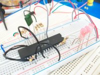
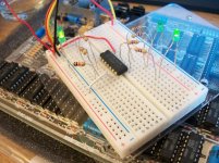
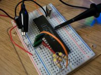
Well, I had to give it a go and run the ULA for itself on a breadboard, it still run really hot!, measuring it it uses 440mA, but 120mA or so of that is going through those resistors. So let's say 320mA, so that's ~1.6W!? [But this might be normal?, from reading this thread on another forum]. The clock output is still working, so now I have to find a way to test the other features.

100_3053.jpg

Anyway, just a tiny update.

Cheers!,
Adrian.
 
So I've been studying the schematics a little, the little core next to the DC-jack is apparently part of the PSU that generates all the voltages required apart from the +5V. They include +/-12V and -5V. I have seen some NOS coils so that could be an alternative.

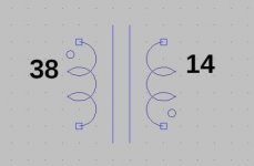
Does anyone happen to know what the rating on that coil is?, in the schematic it says just says 13 and 39, so that could be turns or uH. So I probably have to find a way to feed the board all the required voltages during testing. Trying to reconstruct a little switching mode supply before you know the board works at all... yeah :p

Cheers!,
Adrian.
 
Last edited:
Borrowed a DSO today and did some poking around, it seems like the ULA might be somewhat alive?

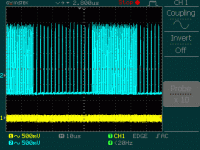
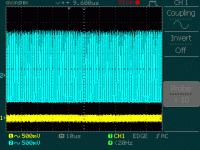
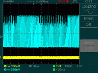
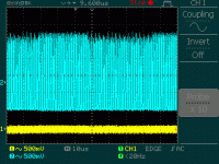
First test was to see if it did the notorious clock stretching thing when the address is in the video ram space:
clock stretch A14=Hi A15=Lo.gifclock output A14=Lo A15=Hi.gifclock noise A14=Lo A15=Lo.gifclock noise A14=Hi A15=Hi.gif
All the four states of A14 and A15, so you can see it is only doing the clock stretching when A14 is High and A15 is Low. There's noise when they're in the same state, both High or both Low. This might be because it's running on a breadboard with a lot of unconnected pins?

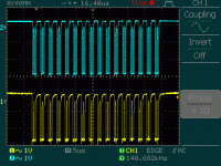
Next test was to see if it did CAS and RAS:
cas and ras output.gifcas and ras output longer time div.gif
It does!

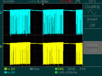
I also had a look at the video output, to see if there were some sync running:
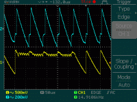
video gul = y blå = v.gifvideo gul = y blå = u.gif
In order the traces are: Yellow = Y and Blue = V, Yellow = Y and Blue = U. The Y and U was after a few attempts to capture the pulse I saw from time to time.

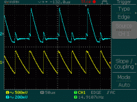
And just to do a last check I had a look at the clock division again:
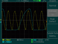
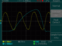
clock dividing 2.gifclock dividing.gif
It's the wrong x-tal but it's dividing it in half two times, as it should :)

So that's a little update, it doesn't seem completely hopeless. Still have made no real progress on the PSU reverse engineering, but this might take a while. As I said before, the ULA being functional is the most important part of this repair project.

Cheers!,
Adrian.
 
Last edited:
Well, I did it! I unwound what was left of the coil. Curiously it seems like the numbers given by the schematics are the number of turns. I got it to 38 turns for the outer windings and 14 for the inner coil. Now I'm not confident that it was exactly 14 since a few turns were under the broken coil.

100_3094.jpg

The ferrite core inner diameter is 3mm and about 3.5mm tall. Wire diameter is about 0.3mm, checking with my calipers.

inductor.jpg

The dots mark the last turns ending point. In reference with the DC plug above.

Looking from the top, the connections are:
Left side (38 turns) Top: R61, Bottom TR4: Base.
Right-hand side (14 turns): Top: 9V, Bottom TR4: Collector.

However the schematics have the number of turns the other way around. It's apparent that the coil have been de-soldered, so someone might have done a real bozo move. Sigh...

So yeah, I don't know. This board probably should be abandoned?, if things have stopped checking out already.

Cheers!,
Adrian.
 
Back
Top