• Please review our updated Terms and Rules here

Mariposa SRAM Card?

sponaugle

Member
Joined
Jan 30, 2019
Messages
26
Location
Portland, Oregon, USA
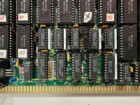
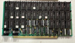
Is anyone familiar with this S-100 64K SRAM card?
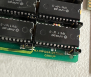
It says "Mariposa Design Group" on the side, and has 64K of SRAM. Each SRAM has a small jumper that is labeled RA/RO (Read Only?).

The center of the PCB has a set of 4 jumpers labeled X0/G0 to X3/G3. Another jumper labeled GB, and another labeled EX. Near the bottom there are 8 jumpers for A19-A23, I assume to allow this SRAM to be places higher in memory in a system with 20 or 24 bit address bus.

This was is in an IMSAI 8080 I just got, but there were a number of cards that I think may have just been installed to store them. (3 different floppy controllers for instance). Would it be expected that this RAM card would have support for the PHANTOM signal?

The CPU card in this box is the Cromemco ZPU Z80 with the jump start set to 0xF000, and one of the floppy controllers has as ROM at 0xF000, so I assume the SRAM card would need to support the PHANTOM signal?

-Jeff
1698765363879.png

1698765485107.png

1698765585279.png
 
Is anyone familiar with this S-100 64K SRAM card?
It says "Mariposa Design Group" on the side, and has 64K of SRAM. Each SRAM has a small jumper that is labeled RA/RO (Read Only?).

The center of the PCB has a set of 4 jumpers labeled X0/G0 to X3/G3. Another jumper labeled GB, and another labeled EX. Near the bottom there are 8 jumpers for A19-A23, I assume to allow this SRAM to be places higher in memory in a system with 20 or 24 bit address bus.

This was is in an IMSAI 8080 I just got, but there were a number of cards that I think may have just been installed to store them. (3 different floppy controllers for instance). Would it be expected that this RAM card would have support for the PHANTOM signal?

The CPU card in this box is the Cromemco ZPU Z80 with the jump start set to 0xF000, and one of the floppy controllers has as ROM at 0xF000, so I assume the SRAM card would need to support the PHANTOM signal?

-Jeff
The board schematic can be found here:

The board had jumpers for:
- each memory chip socket, allowing for a choice of either a RAM or a ROM chip to be placed in the socket
- selection of on- or off-board generation of MWRITE
- selection of extended addressing (A16-A23)
- selection of the memory block, or the entire board, that would respond to PHANTOM
Thanks so much!... I missed that location for looking for the manual or schematic. Sweet!

One other somewhat related topic - I believe there are subtle difference between a system that has an 8080 vs one that has a Z80 in regard to RAM boards. One of the dynamic ram boards I have has a dedicated jumper for selecting 8080 vs Z80 ( A CCS 2065). On that board the jump selects between using sMEMR (Z80) or pDBIN(8080) as an indication of a read operation.

Looking at this schematic for this board(the Mariposa), it uses a NAND gate with both sMEMR and pDBIN to trigger a read, which I *think* would work with both the Z80 and the 8080, since the problem on the 8080 is subsequent reads not taking sMEMR back high the low. Am I interpreting that correctly?

Jeff
The purpose of the sMEMR signal is simply to indicate the current bus cycle is a "memory read" cycle. If back-to-back bus cycles are both MEMR cycles, there is no reason MEMR has to change states between cycles per the IEEE696 spec for the S100 bus. Some Z80 boards are designed to have sMEMR change state between all bus cycles even back-to-back MEMR cycles - but strictly by the IEEE696 spec that is not mandatory.

pDBIN is the actual bus control signal that tells an addressed peripheral (like a RAM board or a data input port) to gate data onto the bus during a read operation. Since pDBIN is active for both a "memory read" and an "input port" read cycle, it is always necessary for a RAM board to qualify pDBIN with sMEMR to gate data onto the bus during a memory read operation, irrespective of the type of CPU. Even on the CCS2065 dynamic RAM board, the data bus driver's output is determined by pDBIN qualified by that board's internal "board select" signal.

Dynamic RAM boards have complex timing requirements. These boards benefit from being able to determine, as early as possible in a bus cycle, if (for example) a MEMR cycle should be initiated. The CCS2065 is designed to take advantage of the way many Z80 boards were designed which was for sMEMR to always change state even between back-to-back MEMR cycles, hence the board can determine when a new sMEMR cycle is starting. Since sMEMR goes active well before pDBIN, a DRAM board can optimize its timing by taking advantage of this advance notification that MEMR cycle is occurring. With an 8080 (or many other CPU boards) sMEMR may not change state between back to back MEMR cycles and has to using pDBIN instead, with less optimal timing.

Static RAM boards have far less complex timing requirements than DRAM boards. The board's RAM chips start their access cycle as soon as their address inputs are stable with no need to look at any other S100 bus signal to initiate the cycle.
Ah yes, that makes complete sense! I was not considering the need to generate the RAS/CAS signals on the dynamic RAM board, and the somewhat tight timing that implies. Thanks for the detailed explanation. I thought the refresh technique used on the CCS2065 was pretty interesting, being able to squeeze in the refresh at the end of an M1 cycle, and even during long wait state cycles. Lots of interesting things in this S-100 world. ;)
 
A good static memory board schematic to look at is the Standard 16k board from Seattle Computer products.

They used the absolute minimum number of control signals to make a static board work in an S-100 system. That board design helped me figure out what minimum signals I needed to interface other experimental S-100 boards to the bus in my SOL-20, like the Light pen board I made and the connections shown on page 4:


www.worldphaco.com/uploads/LIGHTPEN.pdf
Thanks Hugo. I'll take a look!
 
Back
Top