• Please review our updated Terms and Rules here

Model 3 - Double-wide Bug - Solved?

Joined
Jan 28, 2025
Messages
34
I have been looking into the Model 3 and its video generation, and specifically its ability to De-Glitch. During this research I came across this article

Double-wide Bug
http://48k.ca/bug32.html
George Phillips, October 5, 2009, george -at- 48k.ca

It talks about the an issue in the Model 3 where --- "If the display is in double-wide mode (32 x 16 characters),
And the processor reads or writes video memory, Near the time the video circuitry is reading video memory,
Then the next RAM access by the processor will be corrupted.
" --- but offers no solution.

So is this (the following) the reason ? First off I don't think it is related to 32 char mode specifically, here are my thoughts

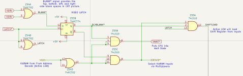
First lets go back to whats happening, memory access is being corrupted by Video Ram (I will abbreviate to VRAM) , how does this occur. The following is the buffer which buffers VRAM onto the Data bus. The important point is the controls are by VRD* and VWR*. Where do they come from.
2c2beba3-01b3-379a-7fd6-9c6d5f38edfd

These come from one of the multiplexers that selects the address/control lines (inputs) to the VRAM. You can see the VRD* and VWR* signals here, the top inputs are from the video circuitry (note how the VWR and VRD are selected as HI, basically disabling the above buffer), and the bottom input come from the CPU. Note the S line (not shown) comes from RSVID*
48254de6-6a52-819f-25e8-1ec18d7b5859

RSVID* comes from the below logic, in summary it takes two inputs, VID* - (address decoder for VRAM), and PBLANK* (is Video currently in one of the blanking intervals)
and produces 2 opposing outputs
  • PWAIT* - put the CPU into a wait state basically since the VRAM is needed by Video generation
  • RSVID* - buffer the VRAM to the CPU, turn video RAM over to CPU BUS.
Sounds logical I guess. I am guessing the JK flip flops (on the inputs) are needed to hold those signals as input for the length of time needed to process the access request.
  • LATCH - is the signal that loads the VRAM buffers (from RAM before the bits are shifted out)
  • CLOCKP - So what is CLOCKP ?

04430700-1c86-30ba-064d-3fbf2c8b1cc0

This is where it gets interesting.
If you read the The gate on the right (below) is an OR gate with negating inputs - The CLOCKP is multiplexed from one of 2 signals depending on RSVID*
  • if RSVID* is inactive - CPU doesn't have access - (bottom half) then CLOCK. This makes sense the RD / WR signals could change with any given clock pulse. Noting this is the base clock not the cpu clock. But regardless of the CPU asserts a VRAM address onto the Address bus the selection logic (above) needs to know about it.
  • If RSVID* is active - CPU does have access) - (top half) then clock with the LATCH signal ???

cf389dc5-b0af-9c34-e142-d1561b3f1c86

... OK? So what does this mean ...

This means that is CPU currently has control of VRAM the new status of VID* (VRAM address decoder) will not be clocked into the JK flip flop until the next LATCH, which happens when the raster needs to read the next VRAM byte - This could take some time ...

So after CPU has successfully done its VRAM access, The CPU A0-A9, RD* WR* signals will remain connected to VRAM, and of course this is without any address decoding! VID* is no longer asserted,... well that is until the raster needs to read the next VRAM byte. This is why the problem is only observed in 32 Character mode, its simply a case of the VRAM being exposed to the bus for longer.

Simple Solution: Get rid of CLOCKP (and the circuit above), just use CLOCK. In this case what is the purpose of the JK FLIP flop in the first place ?

Make Sense?
 
Looks like the images in your post have gone away.

I need to update my web page. The bug has been seen on other Model 3's but only early revisions of the machine. Tandy fixed it at some point. And the Model 4 circuitry is entirely different so I'm sure the bug does not apply there.

I don't trust my ability to static analyze a digital circuit but what you say seems to make sense. Since the bug was fixed we could verify your reasoning by seeing if the later Model 3 boards correspond to your suggested fix. Or, I suppose, any difference they have from the schematic would suggest a solution.
 
Looks like the images in your post have gone away.

It's a shame they're missing, because good heavens the schematics in the Model III service manual are hard to navigate, at least in scanned PDF form.

Simple Solution: Get rid of CLOCKP (and the circuit above), just use CLOCK. In this case what is the purpose of the JK FLIP flop in the first place ?

... I walked through it myself and, yeah, this is a genuinely baffling design. The only reason I could imagine having a clocked element in this circuit would be if they originally intended a more sophisticated snow removal strategy, like timesharing access to the video memory in-between character fetches so the CPU would spend less time in WAIT? (What I'm picturing here would be something like is an access lands during the active scanline you'd raise "wait" automatically, hold it until the current character fetch cycle has finished, switch the multiplexer to the CPU, fetch the desired character into an output latch, drop WAIT, and reset the on-shot you used to do this when the CPU RD signal goes high again. This would of course need the addition of an output latch and the one-shot logic.) Holding the buffer enabled beyond the rising edges of the CPU's read/write lines on end of the cycle that actually involved VRAM is pretty nutterbutters.
 
In case it has any bearing on the analysis, the video wait states are suppressed when drawing the bottom 4 lines of a non-graphics character. Only the top 8 lines of a non-graphics character are pulled from the character generator ROM. The bottom 4 lines are always blank so there no need to worry about VRAM conflicts since the display wasn't going to show anything.

There's also an issue that if the Z-80 has an access already in progress it will take priority over the video display circuitry. This can lead to blanking on the left edge of the screen and blanking after those bottom 4 lines of a non-graphics character.

I discuss that blanking on this page: http://48k.ca/beamhack5.html
 
There's also an issue that if the Z-80 has an access already in progress it will take priority over the video display circuitry.

That makes sense, given the only ways you could avoid it would be pretty hardware intensive. The timing of video accesses are non-negotiable, and unless you did something really tricksy like cycle-stretching to let you "suspend" the Z80's access mid-flight you're going to have to let it finish. (Another strategy they could have used would have been to implement a state machine so the "wait" logic gets enabled a few character timing positions *before* the active area, thereby giving enough time for any in-flight access to finish before you actually need to start shoveling characters.)

It's still just really weird that they would latch the buffer open the way they did. The direction signal of that buffer could be simply connected the CPU's read or write signal (depending which direction the 74245 is facing) and the enable connected to the decoded video enable line (gated by the wait state logic, of course). I don't see any logical reason for latching it beyond the time the video address is selected by the CPU.
 
I see the images on my desktop machine running chrome. But not on Phone browser. Try the attached PDF which should work.

If you have an affected machine, you could cut a trace and test with a bodge wire.
 

Attachments

In case it has any bearing on the analysis, the video wait states are suppressed when drawing the bottom 4 lines of a non-graphics character. Only the top 8 lines of a non-graphics character are pulled from the character generator ROM. The bottom 4 lines are always blank so there no need to worry about VRAM conflicts since the display wasn't going to show anything.
i disagree with this assessment. The video memory still needs to be fetched for every scan line (in visible field) to assert the 6 six pixels to load into shift register. For characters the ROM has nothing to display, but for graphics the bottom two pixels still come from bits in the byte from VRAM, plus Bit 7 asserts to use graphics. It cant know this without reading VRAM, regardless of the character being displayed.
 
Attached is a screen shot of simplified (untested) logic that I was planning to use in my model 1. It was based on understanding model 3 and article (first page attached) in 80 Micro
 

Attachments

  • VRam-Wait-Gen-New.png
    VRam-Wait-Gen-New.png
    159.4 KB · Views: 3
  • page_290.jpg
    page_290.jpg
    115 KB · Views: 4
i disagree with this assessment. The video memory still needs to be fetched for every scan line (in visible field) to assert the 6 six pixels to load into shift register. For characters the ROM has nothing to display, but for graphics the bottom two pixels still come from bits in the byte from VRAM, plus Bit 7 asserts to use graphics. It cant know this without reading VRAM, regardless of the character being displayed

Page 17 of the Model III service manual says this is what it does. I’ve never owned a III, only Model Is and 4’s, so… if you fill a real III’s screen with graphics blocks that have the bottom 4 pixels white and pound on video memory does it glitch? Seems like an easy test.
 
Page 17 of the Model III service manual says this is what it does.
You are correct, But in a way both of our statements are true.

In case it has any bearing on the analysis, the video wait states are suppressed when drawing the bottom 4 lines of a non-graphics character. Only the top 8 lines of a non-graphics character are pulled from the character generator ROM. The bottom 4 lines are always blank so there no need to worry about VRAM conflicts since the display wasn't going to show anything.

In M3 Blank* signal includes an .. OR (L8 and CHAR) term along with normal VDRV and HDRV blanking - M1 doesn't have this additional term. So on the bottom 4 lines (non graphic) the since blanking is active CPU requests to VRAM will be serviced without wait states.

However in theory, since CPU can gain access to VRAM during non-graphic character (bottom 4 scan lines), and if CPU access still active when video goes to read next character into Buffer, then will reset to 0, displaying nothing. Which is fine if the character doesn't display anything in bottom 4 scan lines however 48 out of the 256 characters will be affected.

I tried this (admittedly in emulated trs80gp Basic) by filling VRAM with alternating graphic an non-graphic characters e.g. ( decimal 32,191) , but didnt see an issue reading back from VRAM in a single line with goto.

Dont have M3 to test properly.
 
I agree with your analysis. I couldn't see the pics either but I was able to infer the parts of the schematic from the descriptions. And yeah the scanned schematics are hard to look at. I also agree that it's not specific to 32 character mode - I'm guessing for a fast enough z80 clock it will also occur in 64 character mode. I'm guessing they wanted to synchronize the switch back to the raster circuits but it's not clear why. I think just switching to CLOCK should work - I'll look for the cleanest way to try that. I also verified the hash on the bottom 4 rows of the graphics characters. I don't know if that was a tradeoff they thought was acceptable or a flawed concept. I didn't know the problem was fixed in later M3's - I have two M3's and both have the problem.
 
I also verified the hash on the bottom 4 rows of the graphics characters. I don't know if that was a tradeoff they thought was acceptable or a flawed concept.
I would guess it was an acceptable tradeoff, and not noticeable under normal circumstances. I guess if you wrote an assemble language program to test for it, the constant cpu access would cause very noticeable issues.
 
Back
Top