Upcoming Events:
- VCF South West - June 14 - 16, Davidson-Gundy Alumni Center at University of Texas at Dallas
- VCF West - Aug 2 - 3, Computer History Museum, Mountain View, CA
- VCF Midwest - Sept 7 - 8 2024, Schaumburg, IL
- VCF SoCal - Mid February 2025, Location TBD, Southern CA
- VCF East - April 2025, Infoage Museum, Wall NJ
-
Please review our updated Terms and Rules here
You are using an out of date browser. It may not display this or other websites correctly.
You should upgrade or use an alternative browser.
You should upgrade or use an alternative browser.
Model 4 Non-GA Garbage at power on
- Thread starter wdatkinson
- Start date
ldkraemer
Veteran Member
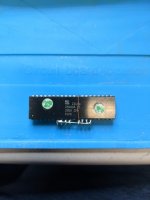
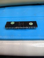
The Z80 (NOP GENERATOR) looks 100% correct. And on your Motherboard the
CPU IC Socket is a 48 Pin IC Socket according to the Tech Manual. The Z80 is
positioned in the Upper 40 Pins, of the 48 Pin IC Socket.
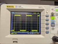
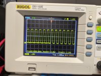
If so A7's square wave should be 1/2 the frequency of the Signal on A6.
Larry
CPU IC Socket is a 48 Pin IC Socket according to the Tech Manual. The Z80 is
positioned in the Upper 40 Pins, of the 48 Pin IC Socket.
If so A7's square wave should be 1/2 the frequency of the Signal on A6.
Larry
wdatkinson
Experienced Member
My socket is a actually a 40 pin.... The remaining pins are till on the board, but empty.
And I'm clear that A7 should be half of A6.... earlier in this thread, I posted the measurements from A0-A6 and all looked good until A7. From A7 on they all measure 520kHz. So what could cause that? Those lines originate at the Z80, right?
I've tracked A6 and A7 through the rest of the on-board IC's until they end. I never find any different values for either.
ldkraemer
Veteran Member
Was the Z80 that you created the NOP GENERATOR a known good Z80 that has been Operational
in a Z80 based Computer?
Let's attack this a bit different. REMOVE the Z80 (NOP GENERATOR). Get yourself a 1K OHM resistor
that is 1/4 Watt. (I = E / R) = 5 / 1000 = .005 (P = I * E) = .005 * 5 = .025 Watts
Lay the resistor Vertical and solder a small wire on the top lead. This goes to the Z80 +5VDC IC socket.
Solder a wire to the bottom of the resistor and this goes to the IC Socket Pin for A7.
Now you have a +5 VDC signal of 5ma INJECTED to A7. Check Address Lines for A{7..15}.
ONLY A7 should be high across your Powered Up Motherboard. Is this what you are seeing?
If so, take a Jumper and connect one end to GND (Pin 29 of the Z80 CPU IC Socket, or GND on
the Motherboard). Connect the Other end of the Jumper to the A7 Pin of the Z80 Socket for A7.
You should now have a LOW Signal injected on A7. See what you have on Address Lines A{7..15}.
If A7 is working correctly, move the wire from the Bottom of the resistor to A8 and repeat the above testing.
What are you seeing?
Larry
wdatkinson
Experienced Member
Ok, so the Z80 is not a known good IC. Principally because I did not have any at the time and no other machine with which to test. Hence I ordered seven of them from a couple of different places on flea bay, hedging my bet that they wouldn't all be bad. All show the same behavior......
So I've got the 1K resistor between pin 11 and pin 37 in the Z80 socket. After the resistor, I'm at 4.7VDC into pin 37. Checking U56 pin 8 yields 4.7VDC. Pin 6 (A6) is 0. Pin 12 of U56 (A7 out) yields 3.4VDC. Once I get to U68 pin 1, I still have 3.4VDC, but I also have it on pin 2 (A6), pin 3 (A5), etc. Following A5 and A6 back to pins 14 and 16 of U56 and I'm still at 3.4VDC.
Before I connect the jumper from U57 pin 37 to ground, I'm leaving the resistor in place and just pulling it to ground, yes?
ldkraemer
Veteran Member
Yes, that will give you a LOW level Signal on the A7 Address Line.
But, you should not have the 3.4VDC on A6 Pin 2 of U68. It should be 0 VDC.
Try Removing U68 = ROMA, U69 = ROMB, and U70 = ROMC, and see if A6 drops to 0VDC.
If it doesn't then something on Sheet 2 of the Schematic contains the problem IC, or it's
U56 that is defective.
Remember that anything above 2.5 VDC is considered a HIGH, and anything less than
around .7 VDC is considered a LOW Signal.
Larry
wdatkinson
Experienced Member
wdatkinson
Experienced Member
wdatkinson
Experienced Member
I failed to mention that in the current configuration (U56, U68, U69 and U70) removed, I still have 1.8VDC on pins 1-8 of the U68-U70 sockets.
ldkraemer
Veteran Member
Let's skip the 1.8VDC on Pins 1-8 of U68-U70 for the moment. (This is unusual, and I don't readily see
anything on the schematics that would/could cause this. You can try unplugging the keyboard to isolate
the A{0..7} lines going to the Keyboard.)
Test U55 Pin 8 which is A8 from the Z80 (CPU) by moving the Wire (HIGH) from A7 (Pin 8) of U56 to
U55. Does Pin 8 (A8) of U55 Toggle HIGH and LOW properly with your jumpers? How about these
Address Lines A{9..15}? Are they correct?
If so, test A9 which is Pin 4 of U55 to see that it toggles properly.
Larry
Last edited:
wdatkinson
Experienced Member
Keyboard is unplugged... Did that a earlier this morning when I pulled U56.
U55 Pin 8 shows 4.7VDC and when I ground U57 pin 38, it drops to a few mV. Same goes for A9-A15.....
U55 Pin 8 shows 4.7VDC and when I ground U57 pin 38, it drops to a few mV. Same goes for A9-A15.....
ldkraemer
Veteran Member
Bill,
OK, the first part is correct. Then you say same for A9-A15. Do they all follow Pin 8 of U55,
or did you test A9 (and it reacted the same, then A10, then A11, then A12, then A13, then A14,
and finally A15)? I'm assuming you tested each A{8..15} one at a time.
Larry
KA0DMJ
OK, the first part is correct. Then you say same for A9-A15. Do they all follow Pin 8 of U55,
or did you test A9 (and it reacted the same, then A10, then A11, then A12, then A13, then A14,
and finally A15)? I'm assuming you tested each A{8..15} one at a time.
Larry
KA0DMJ
wdatkinson
Experienced Member
I moved the resistor to each spot on the U57 socket that corresponds with each address line. I then checked to confirm that the 4.7VDC was present. Then I grounded the line and confirmed that it went low. So A7-A15 I believe are behaving as we expect. I did not test A0-A6 since they were fine when using the NOP generator. The issue I observed started with A7-A15, so I concentrated my efforts on that range. Is that inline with your expectations?
ldkraemer
Veteran Member
Yes, SIR! Now, when U56 is replaced, run the NOP Generator again and see what you get.
Larry
Larry
wdatkinson
Experienced Member
Perfect. Thank you for your perseverance through this process.
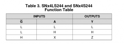
I've ordered 25 74LS244's from DigiKey this morning. So should be 2-3 days with any luck.... I'm looking forward to getting this thing off the bench.... It's HUGE, as you well know.
I've ordered 25 74LS244's from DigiKey this morning. So should be 2-3 days with any luck.... I'm looking forward to getting this thing off the bench.... It's HUGE, as you well know.
wdatkinson
Experienced Member
Well, the 74LS244's arrived yesterday and I was able to replace U56 today. Unfortunately I'm seeing the same results when the NOP generator is back in... 520kHz signals start at A7-A15.... Until I get to A7, they are halved from A1-A6, starting at ~256kHz.
ldkraemer
Veteran Member
Bill,
I found a previous note that David Miltimer had posted about {A7..A15} for the Model 1.
I had forgotten about it, until I was searching for other information.
So, try removing the NOP Generator, Insert the Z80, ROMS, and see if it boots properly.
Larry
I found a previous note that David Miltimer had posted about {A7..A15} for the Model 1.
I had forgotten about it, until I was searching for other information.
The remaining address lines A7-A15 were all measured to be xxx KHZ
David Multimer replies:
The signals on the address lines are perfectly normal.
When a Z80 is hard wired for NOP's the refresh address (A0-A6) will always be the same as the low 7 bits of the instruction fetch address.
So, what you see on A0-A6 is double the duration of the instruction fetch. A7-A15 will go low each and every refresh cycle.
So, the effect of it all is A0-A6 will have a square wave with a 50/50 duty cycle. A0 will have a pulse length that is double the clock, A1 4 times the clock etc.
However, A7-A15 do not follow that pattern because the refresh address counter is only 7 bits.
A7-A15 exhibit a long low which follows the doubling pattern but the high part of the cycle has a series on lows in
it (refresh) that are half the duration of the lows on A0.
Long story short, because of the lows introduced by the refresh cycle (one per instruction fetch) A7-A15 will all read
about double the frequency of A0 which is not changing state during the refresh cycle.
So, try removing the NOP Generator, Insert the Z80, ROMS, and see if it boots properly.
Larry
ldkraemer
Veteran Member
wdatkinson
Experienced Member
My apologies to @David Multimer as I missed his reply.....
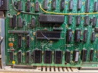
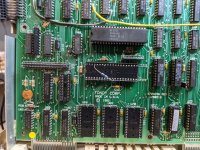
Got back down to the shack this morning and pulled the NOP and replaced the original Z80. I still get garbage on start-up:
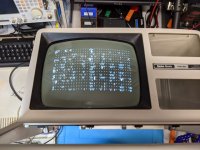
However, upon initial power-on it seemed that the garage was moving around the screen a bit. This repeats on power-cycles. Also the reset button on the keyboard now works, however holding it at power on does not yield M3 BASIC, but more garbage.
So while I still have issues, we appear to have improved things somewhat. Any thoughts on replacing the other 74LS244N?
Got back down to the shack this morning and pulled the NOP and replaced the original Z80. I still get garbage on start-up:

However, upon initial power-on it seemed that the garage was moving around the screen a bit. This repeats on power-cycles. Also the reset button on the keyboard now works, however holding it at power on does not yield M3 BASIC, but more garbage.
So while I still have issues, we appear to have improved things somewhat. Any thoughts on replacing the other 74LS244N?
ldkraemer
Veteran Member
Bill,
The replay from David was years ago and I had saved it in a Note under my Model 1 folder.
Sorry for the confusion.
Try holding down the BREAK Key, and keep it DEPRESSED, then Turn on Power. Release the
BREAK Key when you see characters on the Screen.
If that doesn't work, then try going back over the A{0..15} address lines with the 1K PULLUP resistor,
checking from the Z80 Pin(s) downstream all the way to the Basic ROM(s). Verifying a LOW and
a HIGH on each address Line.
It could also be you have a bad ROM.
Larry

