• Please review our updated Terms and Rules here

Model I No Video

Q2 is getting 5V on it's emitter. The base has 4.2V (or thereabouts, analog meter). The collector, however, has nothing.

I'll look for a source of the MPS3906.

I swapped out the MPS3906 with the new (haha) one and still no voltage on the collector. Dang... thought we might have had it nailed down.
 
@Fooser
Please have a look at Pin 5 of the 75452 as Larry has asked.
Ray

I believe the 75452 is Z41 and thought I'd addressed that in posts 28 and 30. I used a logic probe and pin 5 is low, and pin 6 is high pulsing. Is that insufficient? If so, please be specific. Consider that I am several chapters behind in the book (of things). <grin>

Is there a modern day equivalent for the MC75452P?
 
You should see pin 5 pulsing also, as 6 and 7 are connected together. Which is what I was after when I barged into this thread. Even if Q1 or Q2 were dead shorts, you'd still see a small pulsing voltage on 5. The 75452 is a power buffer--there is more than enough current capability (300 ma) there to overcome the 200 ohms or so that it would see if Q1 and/or Q2 were shorted.

As to a replacement, think cockroaches again. The MC75452P is a Motorola clone of the original TI SN75452. Cheap and ubiquitous--so much so, that they're usually offered in quantity. The current revision is the "B" part, but any version should work just fine in this application.

Any engineer worth his salary knows that the key to quantity manufacturing is to have second sources for components when possible. Otherwise, your production shuts down when your supplier can't get a critical part.
 
Just for grins, I replaced Q1 - just because. No joy. For those TL;DR I previously replaced Q2. I have a replacement SN75452B on order.
 
I replaced Z41 today. No progress. Z41 pin 5 is still low not pulsing, and Q2 collector is still 0 volts.

So far I have replaced Q1, Q2 or Z41.

I have a spare MCM6674 character generator. Should I replace the homegrown one (see pic) and see if that helps?
 
Let's look at the circuit--Q2 supplies the +5 for the open-collector output of Z41. Q2, in turn is driven by Z5, pin 8. This has the effect of "blanking" during the sync interval, which is what you want. So, check Z5 pin 8 to see if it's pulsing.

If it's not, check pins 13 and 5 of Z5, which are inputs. Both should be pulsing.

If you get nothing on Z5 pin 8, try temporarily bridging the emitter and collector of Q2. I'll wager that you'll see a pulse train on the video output.
 
Last edited:
Don,
If you go back to the the Pins 3 & 2 of Z30, you should see either Pin 3 Toggle when TEXT Characters are shifted to the output, or Pin 2 when
Graphic Characters are shifted to the output. If you have the shifted signals here, then check Pin 1 of Z30 to see if you have the Signal
there.

Z10 is the TEXT (8 Bit) Shift Register for TEXT, and Z11 is the Graphic (8 Bit) Shift Register for GRAPHICS. The output of both of these
shift registers is Pin 13. You should have a signal there.

If not, then check Pin 15 of each shift register for the shift signals. The data to be shifted through the shift register is coming from the
Character Generator Z29 (MCM6670 or MCM6674).


Larry
 
Let's look at the circuit--Q2 supplies the +5 for the open-collector output of Z41. Q2, in turn is driven by Z5, pin 8. This has the effect of "blanking" during the sync interval, which is what you want. So, check Z5 pin 8 to see if it's pulsing.

Chuck,

If it's not, check pins 13 and 5 of Z5, which are inputs. Both should be pulsing.

If you get nothing on Z5 pin 8, try temporarily bridging the emitter and collector of Q2. I'll wager that you'll see a pulse train on the video output.

Z5 pin 8 is high and pulsing. Pin 13 is high NOT pulsing. Pin 5 is low and pulsing.
 
Last edited:
Don,

If you go back to the the Pins 3 & 2 of Z30, you should see either Pin 3 Toggle when TEXT Characters are shifted to the output, or Pin 2 when
Graphic Characters are shifted to the output. If you have the shifted signals here, then check Pin 1 of Z30 to see if you have the Signal
there.

Z10 is the TEXT (8 Bit) Shift Register for TEXT, and Z11 is the Graphic (8 Bit) Shift Register for GRAPHICS. The output of both of these
shift registers is Pin 13. You should have a signal there.

If not, then check Pin 15 of each shift register for the shift signals. The data to be shifted through the shift register is coming from the
Character Generator Z29 (MCM6670 or MCM6674).

Larry

Larry,

Z30 pin 3 is low and pulsing. Pin 2 is just low. Pin 1 is high and pulsing.

Both pins 13 of Z10 and Z11 are low and pulsing.
 
Don, we're zeroing in on the problem. If you test a bit, both sides of R29 should show a pulse. Also, my copy of the Model I schematics shows Q2 as an MPS3904, which is wrong. It's a MPS3906/2n3906 PNP transistor. Note that the collector of this transistor goes to R28 and the emitter goes to +5. What this means is that every time the output of Z5 (pin 8 ) is pulsing low, Q2 conducts and +5 should appear at R28. If this isn't happening, I can think of several possibilities, all simple:

1. Q2 is the wrong transistor
2. Q2 is inserted backwards
3. +5 isn't getting to the emitter of Q2
4. Q2 is bad.
 
Don,
Other possibilities are cold solder joint (possible), Open resistor (unlikely), or a cracked circuit trace. CHUCK is right on, it should be easy.
Once you find it, it will all make sense.

Larry
 
Don, we're zeroing in on the problem. If you test a bit, both sides of R29 should show a pulse. Also, my copy of the Model I schematics shows Q2 as an MPS3904, which is wrong. It's a MPS3906/2n3906 PNP transistor. Note that the collector of this transistor goes to R28 and the emitter goes to +5. What this means is that every time the output of Z5 (pin 8 ) is pulsing low, Q2 conducts and +5 should appear at R28. If this isn't happening, I can think of several possibilities, all simple:

1. Q2 is the wrong transistor
2. Q2 is inserted backwards
3. +5 isn't getting to the emitter of Q2
4. Q2 is bad.

I replaced the MPS3906 at Q2 with a 2N3906 just in case I had a bad one. I verified EBC insertion with another working Model I for correctness. +5 is getting to the emitter of Q2. The Q2 base side of R29 is high, no pulse. The other side of R29 is high and pulsing.
 
Don,
Other possibilities are cold solder joint (possible), Open resistor (unlikely), or a cracked circuit trace. CHUCK is right on, it should be easy.
Once you find it, it will all make sense.

Larry

I touched each side of R22-R29 to the soldering iron. I visually inspected the traces and could see no open. If there is a cracked trace, what path should I follow?
 
I replaced the MPS3906 at Q2 with a 2N3906 just in case I had a bad one. I verified EBC insertion with another working Model I for correctness. +5 is getting to the emitter of Q2. The Q2 base side of R29 is high, no pulse. The other side of R29 is high and pulsing.

...and there is why you have no video. +5 isn't getting to the OC output of the 75452. What happens if you short (temporarily) the base and collector of Q2? You should get video output. You could also short the base and collector of Q2, or at least bridge them with, say, a 220 ohm resistor. All you'll be doing is bypassing the blanking circuit. Output will have retrace lines.
 
Don,
"Pin 13 of Z5 is high NOT pulsing"

BOTH, Pins 5 & 13 of Z5 should be low, with a high going pulse.

It looks as if you have no Horizontal Drive (HDRV* at Pin 13 of Z5) to Z5 74C00 . Start with Z6 74C04 Pin 12 and see if you are getting a LOW Pulsing Signal there.
If so follow to to the right until you get to Z5 Pin 13.

You can also do the same for Vertical Drive (VDEV* at Pin 2 of Z57 74C04) to Z5 Pin 5 74C00. Again follow it to the right to Z5 Pin 5.

The Sync Signal needs to pulse for HDRV* OR VDRV*, but not BOTH TOGETHER. Q2 is a PNP and needs a less positive
on base (negative) to turn it on.


Larry
 
Last edited:
Don, I think we are saying the same thing, only different ways. A picture is worth a thousands words when troubleshooting.
That is why I prefer an O'Scope to see the picture of the signal versus a Logic Probe.

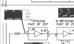
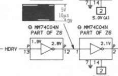
I've zoomed to 400 for two pictures with the signals for HDRV & VDRV from the SAMS Photofacts for Model 1.

This is what you should have, and you need to chase it through to the output of Z5 (Pin 8). You should find one gate
that isn't switching, making the output a HIGH Level.


Larry

VDRV.jpg HDRV.jpg
 
Back
Top