I've been reading up on Multibus and it's beginning to feel like either I'm overlooking the obvious or I'm looking for something that doesn't exist.
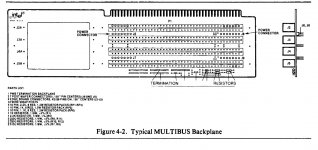
The Intel spec labels the backplane connectors as J2, J3, J4, etc for P1 and J2A, J3A, J4A, etc for P2, with the lowest number furthest from the termination resistors.
But what I can't find is a scheme for identifying the slots. As in, when you're looking into a card cage and somebody is telling you which slot to stick a board into, how would they do so?

